A random question. Since there is some amount of address space below $8000, is it possible to make a cartridge without a mapper, with a 64K ROM chip that will be partially accessible? Of course, more than 16K of a 64K chip will be wasted, that would be unacceptable in 1980s, but today I think it can have some good use, given it wouldn't require too much extra hardware (otherwise a mapper could be used). More specifically, C programs would benefit from having few extra Ks of linear address space, this would allow to have more code and data without need to going low level to do bankswitching.
And a sub question. Are there mappers that have a fixed 32K bank and only switch ROM banks in the lower part of the address space, like $6000..$7fff?
To get 40 KiB of linear address space from $6000-$FFFF, you'd need to make a decoder that returns 0 when PRG /CE is low or when M2, A14, A13, and A12 are high. Such a circuit would look a lot like a PRG RAM decoder.
It's just that emulators don't support it because no licensed game from the early NES era uses this configuration. Licensed games were more likely to use CNROM and read back map data from unused CHR banks, like in Milon's Secret Castle. MMC2 switches $8000-$9FFF and leaves $A000-$FFFF fixed, but only one game ever used that. If you want to switch $6000-$7FFF and leave the rest of the address space fixed, and you want something compatible with emulators, your best bet is FME-7 (#69).
I read somewhere that MMC5 can use $4020...$5fff too. Is it correct?
Since APU registers are internal to the CPU, my wild guess was that you don't need to disable ROM for $4000..$401f. This would allow to have 48K, having pretty simple decoder that only disables first 16K of a 64K ROM, for addresses below $4000.
FDS and MMC5 put registers in that space. But if you want to decode all of $4020 to $5FFF, you need to bring all PRG address lines, A5 through A14, into the decoder. This becomes expensive to do with discrete logic, and by that point, you might as well use CNROM with CHR ROM readback.
Even if APU registers are internal to the CPU, you're still likely to get a bus conflict somewhere. Otherwise, we would probably have already seen such a simple decoder used by unlicensed commercial games.
I have strong doubts about the 'we would probably seen it already' argument. The thing is that at the time when wasting 16K of a 64K ROM became acceptable (near the last days of NES, I think), quality standarts for NES games were really high, with much larger ROM sizes and complex mappers being widely used. So such small improvement could be simply unclaimed.
I already tought about this. Super-NROM with 40kb of PRG ROM is most certainly possible, and would make a lot of sense today.
However, you have to think that back in 1986 to achieve this you'd need :
- a 32k PRG-ROM chip
- a 8k PRG-ROM chip
- a 74HCxxx chip to decode adress for the 8k PRG-ROM chip
- a 8k CHR-ROM chip
While CNROM would have more space overall with less chips, you understand while the overhead of bankswitching was cheaper than the overhead to decode adresses in $6000-$7ffff
Of course you could also get almost 48kb of ROM at $4018-$ffff, but the decoding would be even worse since it would be imperative to block all adresses $4000-$4017 to prevent conflicts with the CPU itself, and this would need several chips to decode.
The question - is it really needed to block $4000..$401f. I recall a discussion of the cloned APUs with switched duty cycle values, with the problem that we can't write APU registers outside of the chip (to use it in a HW player and put corrected data there with some other CPU). I guess there will be no side effects for writes into the area if ROM is enabled. There is only one readable register in the area, and we can put certain values into the ROM at the location to make bus conflict (if it is there) predictable.
I don't know the HW well, so I would like to hear from people who really know that stuff, if this correct and if this doable.
My guess is programmers got over the 32KB hump early by bankswitching so they never considered this because they always used bankswitching and it works. That and mainly Nintendo never offered such a mapper so it was basically a non-option. That and they weren't coding in C like yourself so it might not have been as much of an issue for them as it is you.
The $4020 to $5FFF is basically a non-option based on how many inputs you need. You could do it but with that many pins why not do something more useful. It gets messy to do with discrete ICs which is probably another reason it was never done. One could come up with a discrete design but it's so much easier and defiently more versatile to use a $1-2 CPLD IMO. You could even bankswitch the $6000-7fff between two 16KB pages so you'd have an opportunity to make use of that space. Although it kinda defeats your goal of having more fixed banks...
I don't have any issues with programming in C and/or bankswitching. I don't have any goals here. I just have a simple random idea that could be handy if it is possible to implement.
Currently it is narrowed down to the question: do we really need to block the area $4000..401f? What kind of problem is there if it is not blocked?
Shiru wrote:
Currently it is narrowed down to the question: do we really need to block the area $4000..401f? What kind of problem is there if it is not blocked?
Your controllers and sound wouldn't work...
EDIT: you'd end up with bus conflicts and you'd basically the ROM would be fighting to read/write a different value than desired. So assuming the ROM would win a few of the bus contentions the sound and controllers would be broke.
EDIT 2: (sorry it took me a bit to realize I was ninja'd)
Quote:
I guess there will be no side effects for writes into the area if ROM is enabled.
It depends, you'd have to disable the ROM during writes to prevent bus conflicts which is not normally done with 'NROM' but you could add the logic to do so fairly easily.
Quote:
There is only one readable register in the area, and we can put certain values into the ROM at the location to make bus conflict (if it is there) predictable.
This is the problem, you can't change or move the value around in ROM. It'll ALWAYS be the value you burn in there. So if you enable both the ROM and the single readable register you'll have the two conflicting who knows what you'll get. You have to block the ROM from outputting at this location.
EDIT 3: (the more the merrier)
Actually there are two registers if you want two controllers...
To expand on what infiniteneslives said, it will work iff you disable ROM on writes and reading from $4015 - $4017. The former is necessary to not cause bus conflicts when writing the sound registers; the latter is necessary to be able to read the joysticks and the $4015 sound status register.
Could you build something that will take all 18 control lines and enable ROM for every single bus-conflict-free address? Yes. a 20v8 PAL is probably the most straight-forward way. But I'm not clear on the utility of having the 21 bytes below $4015 contain ROM, since it's not contiguous.
Could you also put resistors in series with the data lines of the ROM so that the CPU's internal peripherals always win bus conflicts? Probably, but you might run into timing issues.
Oh, I have forgot about the controller registers in this area.
Well, I have a ridiculous 'waste'-style solution on the ROM blocking: throw in an extra ROM. I.e. two 64K ROMs, address lines are connected together. The extra ROM contains flags for every single byte of the address space that enables or disables PRG ROM per location. Since we don't need lowest 5 bits, we can use a 2K ROM as the extra ROM. Of course, this is more like a fun thing to think of, not a very practical solution, but should be doable.
HUH?
If I think I understand what you're trying to explain the huge amount of logic needed to decode that 'flag' rom would be huge. It sounds like a lot more of a waste of decoding/enabling logic and processing than ROM. aka most complex solution you can brew up for a simple task...
No logic would be required, just three ROMs - PRG, CHR, and the extra ROM. The extra ROM would be basically 9th bit ('enable') for every byte of PRG, like D0 of the extra ROM connected to OE or CS of the PRG ROM.
Actually, it starts to look not that impractical, because price of the ROM chip is comparable with a CPLD, but you don't need extra tools to program that ROM, unlike CPLD.
How are the two roms connected to each other?
If you use anything smaller than the PRG ROM you'd need a large amount of logic to decode the 'flag' rom. Basically to use 2KB like you suggested you'd need a large CPLD and/or some sort of processor.
If you used 64KB PRG ROM and 64 KB 'flag' rom then maybe you could use the D0 (or any single data line) to drive /OE of the PRG ROM. That wouldn't necessarily require large amounts of logic. But 64KB of ROM at ~1.50 is still about the same price as a $1.20 CPLD and voltage regulator. You also need a larger PCB for your solution (more $ generally). But yes you wouldn't need a JTAG programmer for your solution.
Either way your solution is crazy though IMO

No extra logic for 2K 'flag' ROM is needed. Address lines of two ROMs could be simply connected to each other with a shift of 5 lines (A0 of 'flag' ROM to A5 of the PRG). We'll have one byte of the flag ROM as enable for 32 bytes block of the PRG ROM.
'Crazy' solutions like this were popular in early 1990s in hobbyist electronics, and this is very simple one comparing to some I saw, like
PAL encoder with signal waveforms stored in a ROM.
Ahh I think I understand how you'd connect the 2KB ROM up now. I didn't get the idea of shifting it to control 32byte chunks.
In that case you're looking at more like $0.40 for the decode flag rom.
With that I'd consider your design INTERESTING vice CRAZY...

Quote:
Currently it is narrowed down to the question: do we really need to block the area $4000..401f? What kind of problem is there if it is not blocked?
I believe if you filled your ROM with $FF values for all those values, it might give the correct results in a NES system if you use NMOS-based memory in your cart, since NMOS technology causes 0s to 'win' over 1s, functionally giving a binary and. Of course, this might give totally different results on a clone system where the CPU is not an NMOS 6502.
...but as other have pointed out here before, even if it works it might be a bad thing to do, as this could create more wear on the circuits.
Then again, I guess the same thing might apply to unofficial 6502 opcodes like SAX (and A and X and store result), and I've never seen any recommendations against using those based on electrical wear, only compatibility. Maybe try building this cart and run it for a year's time to prove it's safe enough? :)
'0' wins because N-Channel transistors, used to connect an electrical line to the 0V, are stronger than P-Channel transistors, used to connect to +5V.
Therefore, in any technology, the '0' should always win, unless your technology uses oversized P-Channel transistors, which is unlikely to happen.
Back to the subject I think NROM, and any non-bankswitched mapper could easily be extended to 40kb, the problem is the iNES header only allowing for 16kb increment.
Therefore, 40kb can happen in hardware but now on iNES, but 48kb can exist on iNES, but not in hardware because of the sound/control regs.
Conclusion -> it's better to move to use a mapper if you really can't make things fit in 32kb.
Bananmos wrote:
Maybe try building this cart and run it for a year's time to prove it's safe enough?
You can run it on your system for a year
Personally I wouldn't touch anything that intentionally causes bus conflicts with a 10ft pole. Just plan BAD design. Shiru's proposal prevents this while it's not conventional it's logically sound so it's just an interesting yet valid solution.
Bregalad, did you read few posts above? There is a fun, but viable solution with three ROMs that allows increase of 16K.
No mappers increase linear address space of PRG, and it is a nice thing to have with existing HLL dev tools.
Or, although it's nowhere near as much fun, you could use a 74'238 or 74'239 to get a 46kB aperture.
There is no need for such an EPROM.
You can always have your adress decoded like :
/OE = M2 * !A14 * !/ROMSEL * (A9 + A8 + A7 + ... + A0)
This will give you linear adress space from $4020 to $7fff (and a second EPROM will handle $8000-$ffff as usual) and this can be done with a PAL/GAL chip easily. You could even probably do the logic to use all $4018 to $7fff.
While I fully agree it makes sense, form a software viewpoint, to avoid bankswitching completely, in hardware it takes less chips (or cheaper/simpler chips) to bankswitch the ROM at $8000-$ffff, which is why that's the way Nintendo did it.
The extra ROM would be basically the address decoder, and used in place of PAL/GAL chip, with an advantage to not require extra programmer device.
Not really follow the 46K with 74238/9 idea, though. lidnariq, could you please explain it? Seems to be a good trade, small chunk of memory vs. PCB size.
Edit: E1 and E2 to A15,A14 and A0-A2 to A11-A13, with one of outputs enabling the ROM, something like that?
I'd designed something, posted it, and then realized it conflicted with the internal PPU and RAM — the design mapped the ROM into everything
except $4000-$47ff. Oops. Fixing that is trivial, but involves another gate; if we're trying for a single IC solution it's lacking.
Let me try again, triple-checked this time, using a 74'85. Unfortunately, this only gets you 44kB ($5000-$ffff).
Code:
M2 -> A3
/PRGSEL -> B2 and ROM A15
A14 -> A1
A13 -> A0
A12 -> A>Bin
ROM /CE <- A<Bout
vcc = B3, A2, B1
gnd = B0, A=Bin, A<Bin
Since the CPU's A15 is inverted for /PRGSEL, the top 32kB of address space would be on the bottom of the ROM and vice versa.
I'm not certain whether the '85 (add an 8 input OR) or '238 design is a better starting place if you're willing to add another IC to increase selecting memory by up to 4kB more. Either way, it sadly feels like diminishing returns.
Oh LOL!

Do you really need that extra 2kB to start f**k around CPLD and PAL? 44kB not enough? This is the main reason of bank switching - good compromise between capacity and simplicity. Keep in mind, when Famicom/NES been released and cost of IC's at the time. Early 80' - 32kB memory were huge space.
I think, goal of an extendend NROM design could be defined as '3 chips only with max amount of memory available'. Three chips are CHR and PRG ROMs + an extra chip, the latter is preferably cheap and compact one.
Since 40K would require decoding anyway, 44K is not too bad. Of course, more would be better, but it seems that the max is only possible to get with a CPLD or an extra ROM as decoder. I think, with all pros and cons the 7485 design wins over CPLD/ROM.
I forgot that /PRGSEL can never* be 0 while M2 is 0, which allows us to get back to 46kB:
Code:
M2 -> A3
/PRGSEL -> B3 and ROM A15
A14 -> A2
A13 -> A1
A12 -> A0
A11 -> *A=Bin*
ROM /CE <- A<Bout
vcc = B2
gnd = B1, B0, *A>Bin*, A<Bin
It's more obvious what's happening now, too: A2..A0 compared to B2..B0 is "how does the number compare to 4?"
* Well, "never" as in it's transiently so at the end of a cycle that addressed $8000-$ffff. While M2=/ROMSEL=0, it'll act the same as though M2=/ROMSEL=1, so any glitching would only happen after reads from $c800-$ffff, should be fast enough to not propagate through the 74'85, and should be after the hold time for the CPU is over.
edit: misread the truth table, needed output to be inverted A11, corrections are *starred*
46K with a single 74xx chip - that's neat. lidnariq, how do you think, could this be considered a reliable design? I'm not an EE, so I can't be sure (can only check logic tables, not edge cases with timings etc), but I would like to promote the idea of extended NROM into practical use eventually, and I like this design the best.
I will like this design after i will see working prototype
Shiru wrote:
46K with a single 74xx chip - that's neat.
Even if it can be accomplished with a single chip, BNROM can get you as much as 512KB, also with a single chip. I can understand this being an exercise you guys are doing for fun, but it's hardly practical when you can get 480KB at the same cost of these 14KB. The memory being contiguous is hardly an advantage, since there are things that can easily be offloaded to different banks, such as music code and data.
Offloading things to different banks requires knowledge of the 6502 assembler, compiler internals, and hardware layer in general. I seen this already, it is a serious obstacle for newcomers. In this case extra 14K is a nice thing to have, without any doubt. Of course, if you are not interested in programming in C (or other HLL) for NES, or in small scale projects, it is impractical, useless etc for you.
Isn't there a different 74 series chip that gets you up to 8MB?
Yeah you could use a 8x flipflop UxROM style to get 8MB but it obviously doesn't meet shiru's goal.
Edit: you'd give up the fixed bank that UxROM generally benefits from. Go down to 4MB and you could get it back with the addition of 8 or gates.
Shiru wrote:
lidnariq, do you think, could this be considered a reliable design?
I'd trust it. I even have all 3 ICs necessary to try it out, but neither data nor a PCB.
There is a possibility that not all 74'85s use the same logic on nonsensical cascading inputs. But all the ones I've looked up just now — Phillips 74HCT85, Motorola SN74LS85, and Renesas HD74HC85 — all have the same truth table for the cascading inputs:
When A3…0 == B3…0, then:
- if only one cascading input is high, all 3 are copied verbatim
- if A=Bin is high, A=Bout is high and the other two are low
- if all cascading inputs are low, both A>Bout and A<Bout are high
- if both A>Bin and A<Bin are high and A=Bin is low, all outputs are low
If there exists some IC where we cannot get an inverting behavior, we can still get the 44kB I mentioned previously.
Seeing as the NES runs at only 2MHz, I strongly suspect the glitching will not be a problem. If you want to make an oversize variant of one of your existing games and have me try it out, I can, but it'll take me a little while.
----
Regarding bankswitching: C compilers *can* be written to deal with bankswitching elegantly. But CC65 isn't there. Without a call graph, you could just get away with putting the bankswitch command before every call; without a data "call" graph, you're basically entirely screwed. Even once you have these call graphs, you still need to do the search to map what data and code goes in what bank, dealing with relocations elegantly. All of these things, while not huge, are still probably a hundred hours of work to add to CC65.
lidnariq wrote:
Without a call graph, you could just get away with putting the bankswitch command before every call; without a data "call" graph, you're basically entirely screwed. Even once you have these call graphs, you still need to do the search to map what data and code goes in what bank, dealing with relocations elegantly.
A call graph like
this one?
I like the idea of the compiler minimizing the bank switching automatically, but this depends completely on the mapper, and for this reason it should be very complex.
I'd rather spend 100 hours improving CC65 to produce perfect code you couldn't tell apart from hand written assembly so I could code all NES games I want in a few hours and never deal with assembly again.
OK I exaggerate a bit but the idea is here.
A problem with CC65 is that it is not a NES compiler, it is a general 6502 compiler. NES has many mappers and specific memory layout, you would need to make a NES branch of the compiler to support these things. Generally it would be good to have many improvements in it, but for now we have things as they are, and it does not seem that there is a chance that something will change much in near future.
As for expanded NROM, there are things (that I consider) to do in order to make it practical:
- iNES format decision. I guess it will be 64K with the same layout as in actual ROM (top 32K, then a gap of 2K, then bottom 14K, then unused space). Probably still mapper 0, with extra memory detected by size.
- A modified emulator to be able to make some (test) software that will utilize the extra memory. Once there is some worthy software, I think authors of other emulators will support it.
- Hardware test.
- Popularizing the idea among homebrew developers and romhackers. Includes creating and publishing PCB layout.
The first thing that can run fairly independently of the rest of the program is audio. In fact, it can run so independently that Super NES games run it on a separate CPU with a separate address space. Loading tile data into CHR RAM is another thing that can run as its own self-contained deal. Perhaps the proper abstraction is to treat each PRG bank almost as a separate, cooperatively multitasked program that's linked up by message passing through shared memory.
As for "general 6502", don't the Commodore 64, PC Engine, Atari Lynx, and BBC Micro's "sideways" bus all use a 6502 family CPU and bank switching?
Shiru wrote:
- Hardware test.
- Popularizing the idea among homebrew developers and romhackers. Includes creating and publishing PCB layout.
I know you guys are working on a design using the 74 series chips. As I see it the biggest obstacle to getting a published PCB is quantity. You can make a prototype PCB fairly cheaply if you accept thicker PCBs. I don't suggest that if you have respect for your 72 pin connector. I've created my own 72 pin connector that has no issue with them. Depending on the design it's possible 60 pin connectors might not be an issue.
Quantity is key for PCB cost and using something like the specialized 74 series design or flag rom is basically only good for that mapper. That's one of the biggest reasons I push for CPLD's, they are EXTREMEMLY versatile. With a well designed PCB you could support NROM through MMC3+ on the SAME PCB. This is my goal with
my MMC3 reproboards, to not have limited mappers. Now to make this mapper with my boards it would require a CPLD, but it'd only be $1.20. Yes it might be $1 or more than a single discrete chip that's design is yet to be proven. BUT if 100's of these PCBs are purchased vice a couple dozen, the CPLD effectively becomes FREE.
I now I hadn't planned to include PRG A11 or A12 as possible mapper inputs because generally no mapper would make use of them. This design would be the exception. If else contributes to a test rom, and emu support (even better yet: a game) I'd consider this mapper serious enough to support on my PCB's. I've been trying to think what to name them for awhile. Call it vain if you'd like but this morning INLROM came to mind.
If you'd like to test something sooner vice later on actual hardware the first easy step is a devcart. If someone whats to write up a simple test rom I can create the mapper and run in on the NESDEV1. It would only take a few minutes with good mapper definitions. Maybe just a rom that verifies all of the new addresses are properly read from with no issue.
I don't mean to take over the design or anything, and I'd support where I could if someone else want to make the discrete or flag rom design. But my guess is there aren't too many other people willing to step up and invest the cash in a substantial number of PCBs to make this a reality. If my proposal offends anyone I'll quietly step down.
In regards to the file format, maybe it's just me but it makes more sense for the added address space to come AFTER NROM's $8000-FFFF. I know it's backwards to how things are actually set up, but when I think about designing the mapper and programming the NESDEV1 it makes more sense. I imagine address $0000 of the physical rom being $8000 of the NES and $8000 of the NES being $0000 of the rom which is the way it is currently. Also as you designed a game with this mapper you'd fill the begining of the file first with the traditional NROM filespace, and then spill over into added memory. I guess we'll have to see what makes sense to someone who'd right the emu support as well. Also the gaps would actually be filled with padding data vice just jumping to 'save' file space. Just denote the size as 64KB in the header as mapper 0.
The same PCB that is needed for this 'mapper' could be used for NROM with few jumpers. I'm pretty sure that there always will be way more NROM finished homebrew games than finished homebrew games that use any mappers (but vice versa for unfinished projects).
I honestly don't see any problem with PCBs prices. Don't know, maybe it is something region specific, and it is very expensive in US, but here in Russia hobbyists produce tons of DIY retro computers and devices with large PCBs, and it is affordable enough with quantifies of tens.
If there is an universal PCB for CPLD based mapper, this does not make discrete logic version obsolete, since you don't need a programmer to program 74xx chip, and you don't need someone to write mapper code for the CPLD as well. Both can co-exist, having many options is a good thing.
It's just that you need to invest a couple hundred dollars to get PCBs that are only a few dollars each. In the past not many people have been willing to invest the required money. Sadly most people willing to invest in PCBs are making repros and they generally choose the $2-4 solution for board, CIC, and case from donors. It's difficult to compete with prices of hacking carts... So far bunnyboy is the only one to keep something like this going with his retro boards.
Well, first things first. There is a lot of things to do before any PCB production, and making a PCB layout won't take too much time to worry that it will have low chances to be used.
So, making clear the ROM format. I think it should be like this (ROM offsets without the iNES header):
Code:
ROM NES length
0000 8000 8000 (normal NROM data)
8000 padding 8800
c800 4800 3800 (extra memory)
Because it is located in the chip that way, so it would be possible to simply cut off the iNES header and burn the binary into the chip.
So we have NROM extended to 3 pages, with the third mapped to $4000-$7FFF (first 2 KiB inaccessible). This can be identified with mapper=0 and PRG size=3. We might as well extend CNROM the same way, no? I'd make a test ROM for this, but how would I emulate it to test it?
I can whip up the mapper this evening and run your rom Tepples. You should be able to do the easy test of $6000-8000 if you denote SRAM in the header, most emus support. (can always test with yggi's pogo cats battery)
Do we want an even 64KB (4 pages) or odd 48KB (3 pages)?
Yes, I think extending CNROM the same way would be a good idea. It is also easy to use with a HLL, since only CHR is bankswitched.
To make 'fullscale' tests we first need to modify an emulator. Since this is a 'chicken or the egg' situation, chances to get an active emulator developer interested in this are low (no software to test against and no reason to bother with yet). So I plan to do it by myself. Hopefully this won't be too difficult, it does not seem so at least.
Since the last quarter of a 64K ROM going to be empty, there is not much sense to store it in an iNES file. On the other hand, a ROM burner software may require to pad it to 64K to be used - don't know for sure.
I wrote a simple test program to see what various emulators do with oversize iNES mapper 0 images.
- Nintendulator and Nestopia always map the first 32kB to the aperture
- FCEUX maps the first and last 16kB to $8000 and $c000 when it's a power of two. The emulated machine crashes when it's 3.
The actual layout on the physical ROM would be
$8000-$FFFF are in addresses 0x0000 to 0x7FFF
$4800-$7FFF are in addresses 0xC800 to 0xFFFF
0x8000 through 0xC7FF wouldn't be addressable, i.e. the padding's in the middle.
I'm still undecided whether the right iNES representation is the contents of the ROM verbatim or the linear 48kB as seen by the CPU. I vaguely feel like the latter is slightly more correct, but the former has the advantage that the interrupt vectors are in the correct place in emulators that truncate to the first 32kB, and just discards the remaining 14kB.
lidnariq wrote:
I'm still undecided whether the right iNES representation is the contents of the ROM verbatim or the linear 48kB as seen by the CPU. I vaguely feel like the latter is slightly more correct, but the former has the advantage that the interrupt vectors are in the correct place in emulators that truncate to the first 32kB, and just discards the remaining 14kB.
Storing the banks in an order that doesn't match the linear order in address space has precedent. Mapper 40, for example, has bank 6 at $6000-$7FFF and banks 4, 5, <switchable>, and 7 in $8000-$FFFF. In addition, having an odd number of 16 KiB units would more distinctly identify this variant of NROM/CNROM/CPROM.
I'll have to try making 8 KiB stubs that allow testing some of these programs on a PowerPak or an SNROM board. It'd switch to bank 1, copy $A000-$BFFF to $6000-$7FFF, copy $C000-$DFFF to CHR RAM, switch to bank 0, and finally jump to the reset code. Either way, there'll have to be a Barbie stub at $FFF0-$FFF9 to guarantee power-on behavior:
Code:
fff0:
sei
ldx #$FF
stx $FFF2
jmp real_reset
.addr nmi_handler, fff0_entry, irq_handler
Shiru wrote:
To make 'fullscale' tests we first need to modify an emulator. Since this is a 'chicken or the egg' situation, chances to get an active emulator developer interested in this are low (no software to test against and no reason to bother with yet).
Not sure if you noticed or not since I ninja'd you on the previous page. But I can easily test this in hardware right now with the NESDEV1. At least that way the emulator could compare to the actual NES, which is really how it should be done to verify proof of concept.
If someone provides a test rom I can run it.
To make test on the hardware we need to write and debug test code. An emulator support is needed to do it.
What about hacking a FDS games that runs code at $6000-$BFFF into your extension of NROM ?
There is also quite a lot of emus which are open souce, so you could easily modify one of them to get the oversize NROM configuration you want.
Also I'd add that if NROM were to have a larger PRG-ROM than 32k, since it would be mapped linearly in the adress space the data should definitely be mapped linearly in the .nes ROM too.
Modifying an open source emulator is exactly what I'm going to do. I just need some time to do this.
Linear layout that corresponds to the NES address space has a drawback that you can't just burn this headerless file into a ROM chip, you need to convert it first - extra tool and knowledge required. Layout that corresponds to the ROM address space is free from this drawback. On the other hand it complicates romhacking, so this is definitely something to think well beforehand.
Huh ?
You'll need two EPROMs anyways because there is no 48k EPROM arround.
What makes the most sense is to have in the iNES file first the 16k that goes in the first EPROM at $4000-$7FFF (but adresses $4000-$4xxx should be blocked by some kind of hardware to prevent bus conflicts - anyways those adresses will still exist in the EPROM and in the iNES files - and then data in the second EPROM at $8000-$FFFF, like usual.
I said it in the very first post - 64K ROM chip with wasted 16K (18K in the latest design).
This doesn't change anything - just that since data is wasted it won't be present in the ROM image. The used 48k should still be present, and linear, in the ROM.
Bregalad, please read the thread. The discrete logic design makes layout non linear, with 32K halves swapped. If it would be linear, there would be no talk about non linear layout at all.
I don't think it changes anything if 32k halves are swapped. The NES can't see the difference, so you won't see a difference when you dump the ROM - therefore it should still be contiguous in the ROM image. You'd have to make it non-contiguous when programing the EPROM though - but that's another story.
That is not another story. That is a very important thing to consider beforehand.
Whether you'll see the difference or not is depends from method of dumping, and dumping itself is certainly way less important thing than burning. You know, you need to make something first to have something to dump.
What we're trying to iron out is whether the $8000-$FFFF data appears before or after the $4800-$7FFF data in an iNES image with three 16 KiB banks. Either way, the PRG part is going to have to be rearranged before burning.
If $8000-$FFFF appears before $4800-$7FFF, then the PRG part is laid out as follows:
Bank 0: $8000-$BFFF
Bank 1: $C000-$FFFF
Bank 2: 2048 bytes of padding, then $4800-$7FFF
In this case, you have to double up bank 2 before burning it to the 27C512 EPROM. Then the EPROM sees PRG /CE as A15, and all is well; reads of $4800-$7FFF come from the doubled-up copy.
If $8000-$FFFF appears before $4800-$7FFF, then the PRG part is laid out as follows:
Bank 0: 2048 bytes of padding, then $4800-$7FFF
Bank 1: $8000-$BFFF
Bank 2: $C000-$FFFF
In this case, you have to move bank 0 to the end of the image and then double it up before burning it to the EPROM.
We can just use the first variant but double up the bank 2 in the iNES image, having 4 banks there. Kind of overdump, but these days extra 16K on a hard disk is nothing important, and the files are usually stored zipped anyway.
Although doubling is a problem for authoring tools, and it is better to simply have all zeroes in bank 2. I mean, it is easier to make an assembler generate a file with padding in the middle rather than make it to double a bank.
I think the right layout is either 64kB, iNES PRG*16=4, and the layout is $8000, $c000, blank, $4000, or 48kB, iNES PRG*16kB, and the layout is $4000, $8000, $c000.
A format that's neither "what's on the ROM" nor "what the CPU sees" makes no sense to me.
Just noticed that I messed up my post with proposed layout. I meant the '$8000, $c000, blank, $4000' layout, of course.
So, we have two options with pros and cons (as I see them):
64K $8000, $c000, blank, $4000
+ corresponds to the ROM, just cut header and burn it
- not straightforward from programmers point of view, that will create some trouble for romhackers
48K $4000, $8000, $c000.
- does not correspond to the ROM, a tool would be needed
+ straightforward
That makes choice difficult. Anyone have a major argument to consider that may make it easier? I only have a weak argument about empty space in the middle of the file, but I don't feel it important enough.
Doesn't the PowerPak not like uneven bank numbers as well? I know it likes things padded but IDK about uneven bank numbers. I realize the support isn't currently there, but when it is what would make more sense.
Now it can obviously be changed but it requires making a special case for this one mapper. For the NESDEV1 host software I assume that the ROM image must be powers of 2. Because in the past if you have a rom image that isn't power of 2, it's pretty safe to assume that your file is broke.
I realize it's a sore thumb and easy to recognize odd ROM sizes to flag you've got these weird mapper/ROM setups. As I see it is just as easy to recognize that a NROM mapper has more than 32KB and say "OH, this must be extented NROM." Same thing with CNROM and CPROM. It just seems like a mess to need these file types to require special operations out of tools that use them.
One other thing that complicates odd sizes is when someone tries to use a rom splitter or something to burn the image onto EPROMs. If this really does become popular IMO you'll make things confusing for novice trying to burn EPROMs.
As I see it the .nes file should be a dump of the ROM. Now it doesn't necessarily have to be in order, but it should be the entire ROM image.
infiniteneslives wrote:
Because in the past if you have a rom image that isn't power of 2, it's pretty safe to assume that your file is broke.
Either broke or too big for the PowerPak's RAM. Action 52's PRG isn't a power of 2.
One could argue that action 52
IS BROKE.
Another minor thing to discuss is how to call extended NROM and CNROM. Should we still call it as normal NROM, like NROM-368, or make a new name to distinguish it easily? Like Extended NROM - ENROM (ECNROM), or maybe Super NROM (but there are SNROM and SROM already), or something else.
I think "Extended NROM" is fine, super also sounds like SNES. But if you want a combo of letters I'd stay away from things that start with E or S. They are too similar to MMC1 and MMC5 boards. Maybe something like NXROM, or NEROM?
For NROM, I'd go with NOROM to match the use of O for oversize in UOROM.
For what to call mapper 3 extended in this way, I'm not so sure. There are two ways to "oversize" that, one involving more than four banks of CHR ROM (implemented in Panesian games) and one like this.
NROM is the only series where there are multiple different letters meaning an equivalent board: SROM, HROM, RROM. Consequently, a board name like "EROM" or "XROM" might make sense.
All later boards were at least 5 characters (some more) and the first letter specified the class; SAROM, EWROM, &c: keeping with this would suggest a board name like NEROM or N4ROM.
NROM is also unique in that it's the only board series which specifies the size of PRG. NROM-128 and -256 would suggest -368. However, there is no such distinction between 16kB and 32kB PRG on CNROM, so if we want the same naming convention extension for both, this won't work. Which is unfortunate, because I like this choice best.
infiniteneslives wrote:
I think "Extended NROM" is fine, super also sounds like SNES. But if you want a combo of letters I'd stay away from things that start with E or S. They are too similar to MMC1 and MMC5 boards. Maybe something like NXROM, or NEROM?
I'd like to help with this. If I understand it you're wanting emulator support for an iNES image that is mapper 0 with 32KB of appended ROM data. The 32KB appended is a repeat of the first 16KB ROM bank [which would otherwise be placed at $0], 2KB of pad bytes, and 14KB of extra ROM that is visible to the CPU at $4800.
I also understand Shiru is modifying another emulator...if you guys have what you need already I'll just add it so I can play whatever games he comes up with in my emulator!

We don't have everything that is needed yet. Still have to settle up on the iNES format for this extension. After this, an emulator would be needed to make a test code to test the design with a hardware prototype, then to create something that would be a reason for developers of other emulators and hardware to bother with adding support for the extension.
So, if you willing to help by adding support into your emulator, this would be great. Just wait until the format will be decided - this is a thing that is better to be well thought.
Shiru wrote:
We don't have everything that is needed yet. Still have to settle up on the iNES format for this extension.
I vote:
64K $8000, $c000, blank, $4000
EDIT: and NROM-368
Shiru wrote:
We don't have everything that is needed yet. Still have to settle up on the iNES format for this extension. After this, an emulator would be needed to make a test code to test the design with a hardware prototype, then to create something that would be a reason for developers of other emulators and hardware to bother with adding support for the extension.
If the iNES header of the NROM-368 file were to suggest that there were 3 16KB PRG banks wouldn't that be all that's necessary--for NROM.
lidnariq: I see nothing wrong with using NROM-368 for NROM to follow its convention and something else for CNROM -- CNOROM?
I just realized that's one letter short of MORONiC!

I think I'll just go add support for loading this extra bank and using it...then when the format is solidified I'll be ready with the back end done.
I don't get the $8000, $C000, blank, $4000 order.
Okay, this is the order you'll have to burn the data to the ROM.
HOWEVER, what really counts is what the CPU sees. I don't care at all how it's implemented in hardware, at least in iNES format.
If could be done with a single EPROM, a combination of 32k + 16k, or a combination of 16k + 16k + 16k, or something even more crazy - it's not my problem.
Therefore the only order who makes sense is $4000, $8000, $C000.
No blank bank or anything since we don't want a dump of a part that is hidden to the CPU anyways.
And if you need to re-arrange before burning due to your hardware implementation of this sheme, sorry but it's something different than the logical concept behind extending NROM.
As I already said you could do it as well with multiple EPROMs, then you would not need to reorder the data, but you'll need to split it apart. Again this is not the problem of the iNES ROM image.
PS : The "Super-NROM" name was originally my idea.
It was not intentional iit sounded like something related to the SuperNES.
Bregalad wrote:
And if you need to re-arrange before burning due to your hardware implementation of this sheme, sorry but it's something different than the logical concept behind extending NROM.
As I already said you could do it as well with multiple EPROMs, then you would not need to reorder the data, but you'll need to split it apart. Again this is not the problem of the iNES ROM image.
PS : The "Super-NROM" name was originally my idea.
It was not intentional iit sounded like something related to the SuperNES.
I agree...emulation and burning are different realms.
This is also my vote for the $4000,$8000,$C000 iNES.
Breagalad, basically your argument is 'I don't like this because it seems illogical for me and like that because it seems logical for me', that's it. This is not something that changes current balance of pros and cons and helps to make a desicion, it just a discussion of a personal view of a problem.
'I don't care' and 'not my problem' are not valid argument, it is not something personal to you that no one else will use.
'What CPU sees' does not counts, because CPU is a thing, it simply works, and 'convinient or not' does not matter for it. It matters for people who will have to work with these files.
Multiple ROMs is not a practical option, the whole point of the extension is that modern electronics allows to make it in an easy way, as a waste of resources is acceptable these days.
NROM is kind of a format for beginners, requires less knowledge and skills. Extended NROM is targeted to the same category, to the people who not yet care or know tricky hardware details etc. It should be easy to use for all purposes, including ROM burning. Otherwise other people will have to answer endless questions like 'I did the same as I do for NROM games, but my cartridge does not work'.
Bregalad wrote:
I don't care at all how it's implemented in hardware, at least in iNES format.
Don't forget that hardware uses the iNES format.
I'm not saying I won't support the odd sized iNES file with the NESDEV1. But when you consider how to handle rom images with PC tools it makes things super nice and clean if you can assume even ROM sizes. odd sizes require special cases and such which would be nice to avoid. I know it doesn't sound logical. But personally I think we should put heavier weight on what's better and more convenient for emulators, ROM tools, and hardware. To most people they would never know the difference between the two choices other than it might not be sound logical to you.
To me order doesn't really matter in implementation. I see valid reasons for both choices. Neither has significant drawback IMO.
cpow wrote:
I agree...emulation and burning are different realms.
EDIT: Devcarts are stuck in the middle of those two things.
Ok, shiru's proposal would make the burning process easier, it's true. However it would make the compile process harder to have to reverse the data order.
The only goal to have ROM linearly mapper to space without using bankswitching is so that you can code something without caring where it will fall in memory, and that you can have some routine starting at $7Fxx and continue into $80xx. Therefore there is probably no way to tell the compiler to reverse the bank order in the final file in a single pass, unless you split it in two banks, and this kills the main purpose of having the ROM mapper linarly in the first point.
Therefore you'll need another "tool" to build the iNES ROM, there is probably 9128 ways of doing it, but in all cases it will complicate the building process to simplify the burning process.
This is not necessary a bad thing, but I just want to make sure you guys are aware of that.
The order $4000, $8000, $C000 makes simple building process, but complex burning process, and makes the most sense. The order $8000, $C000, blank, $4000 complicates the building process and makes a little less sense, but simplifies the burning process.
EDIT : Anyways this is the 89478276th thread with debates about mappers, board and hardware. Yet all the better homebrew games so far uses plain NROM and it works just as well if you ask me - and there would be a LOT of room for anything even if you restrict to existing mappers.
Now that's a good argument and reasoning, thanks.
I thought about it, but not too deep, as I get used to assembler's abilities to swap banks in the resulting file in a required order. However, I forgot that CC65 would probably need to have a large linear chunk for the code segment and will not be able to spread code over two segments automatically.
So what is needed is to figure out - if it is possible to make CC65 make the data swap in the resulting file using memory config file only, without external tools.
I don't consider other assemblers, because larger linear space not really needed for users of these, and there is probably a workaround with using few banks/sections anyway.
Regarding importance of the NROM extension in general - yes, it is not very important, but it is a nice small improvement that is (relatively) easily achievable. As an author of a few NROM games I can tell that there is almost always shortage of room, especially if the program is in C. Also, one of the most often asked improvements for games is 'more levels'. More levels - more room needed - in case with C easier to add with extra linear space.
Bregalad wrote:
Yet all the better homebrew games so far uses plain NROM and it works just as well
How much of this is due to developers scaling back the scope of their projects due to 1. lack of artistic resources and 2. lack of battery-backed or IRQ-capable reproduction boards?
Shiru wrote:
there is almost always shortage of room, especially if the program is in C.
Of course, one thing you could do is look at the resulting assembly code, rewrite the most space-inefficiently compiled parts, and submit them to the cc65 project.
Shiru wrote:
Now that's a good argument and reasoning, thanks.
I thought about it, but not too deep, as I get used to assembler's abilities to swap banks in the resulting file in a required order. However, I forgot that CC65 would probably need to have a large linear chunk for the code segment and will not be able to spread code over two segments automatically.
Usually you don't use the compiler, linker, or assembler to do the "built executable to burnable binary" manipulations. I use objcopy to do that. If there's similar in cc65 toolchain or if GNU objcopy could be used then there's no need to debate the complications of how to take a linear image and make it burnable nonlinearly.
cpow wrote:
If there's similar in cc65 toolchain or if GNU objcopy could be used then there's no need to debate the complications of how to take a linear image and make it burnable nonlinearly.
Except that much of the reasoning you guys have in favor of this cart is that newbies get a larger linear space to work with. What's the point in that if compiling/assembling gets considerably more complex? Your average NESASM/ASM6 newbie will hardly understand this. Seriously, offloading the music engine/data to another bank sounds much simpler.
tokumaru wrote:
cpow wrote:
If there's similar in cc65 toolchain or if GNU objcopy could be used then there's no need to debate the complications of how to take a linear image and make it burnable nonlinearly.
Except that much of the reasoning you guys have in favor of this cart is that newbies get a larger linear space to work with. What's the point in that if compiling/assembling gets considerably more complex? Your average NESASM/ASM6 newbie will hardly understand this. Seriously, offloading the music engine/data to another bank sounds much simpler.
I'm confused. I was arguing exactly the opposite. Compiling/assembling/linking has *nothing* to do with preparing the linked-thing to be burned in whatever device(s) it'll end up being burned in. Heck, you could even accomplish whatever's necessary with something like head/tail.
Your average newbie won't have to understand how to make a burnable image, right? They'll just have to understand "I get an iNES out that is runnable in emulator x, y, or z..." Once they get to the point of wanting to burn something they'll probably be considerably less newbie-ish.
Since there are many ways to do it, my design approach is to find a solution that will simplify as much things as possible without involving any extra knowledge and tools than required to handle not extended NROM files.
If a compiler can rearrange data to make a ROM image that is easily burnable without extra tools and without complicated programming, it is a win, and this solution is the best.
I honestly don't get the attitude 'I don't understand/don't need/don't like it, so it is useless/bad/not needed'.
Also, please, guys, don't tell me how I can solve my personal problems I mention in the thread, like shortage of space in my projects, or handling mappers, offloading data into banks etc. Be sure, I know how to do it, is capable to do it, and in fact did it in the past. My interest in extending NROM and my point of view on its design is based off my desire to bring more people on the platform by lowering the entry barrier in various ways, and also based off my experience of communication with these people.
cpow wrote:
I'm confused. I was arguing exactly the opposite.
Oh yeah, my bad! =)
At this point, if kevtris doesn't have anything to say, I'm inclined to go with tokumaru's suggestion and define no-mapper PRG ROM as always having the banks in linear-address-space order because of the noob-friendliness advantage.
- 1 bank: mapped into $8000 and $C000; optional PRG RAM at $6000
- 2 banks: bank 0 in $8000 and bank 1 in $C000; optional PRG RAM at $6000
- 3 banks: bank 0 in $4000 (first 2048 bytes inaccessible), bank 1 in $8000, and bank 2 in $C000; PRG RAM forbidden
As for burning an EPROM, one needs a tool anyway to split an iNES file into header, PRG, and CHR. A tool supporting this format extension could have an option to rearrange PRG into 1, 2, 0, 0 order for an EPROM image.
(Note to self: Try to catch kevtris on EFnet tonight.)
I'm starting to think the 'in order' method is the better choice too:
$4000, $8000, $c000
Are there any arguments to go with 3 banks vice 4 aside from waste of space? Not to discredit the space argument but it's the only one I've heard. However I agree with Shiru that it's kind of a moot point.
I'd prefer a format with:
blank, $4000, $8000, $c000
Odd banks will be annoying but not difficult to add a special case for in my software/hardware. I guess I'm just more concerned about the idea of odd bank being acceptable or the norm. So really my argument is that there should ALWAYS be even (power of 2) number of banks. Moving files around is simpler and potentially quicker if you don't have to make special cases of when there are odd ROM sizes. I don't know what's all involved with the powerpak but with the NESDEV1 I've got a small 8bit mcu that's handling these special cases. Add this one mapper and it's not much issue. But if down if the road all kinds of special odd ROM sizes need to be supported it'll be a headache. Especially if one setup puts the padding in front or in the back. Then there are even more special cases. I guess I see leaving the blank bank out as somewhat ambiguous from the perspective of how the mapper interact with the ROM. And there are already enough ambious things with iNES that I'll argue against adding another until people agree or they just tell me to shut up.
I would think it would also be easier if down the road someone wanted to bank swap the lower memory that's being wasted here. Seems somewhat logical to me if one only stores level data and/or music there. The change becomes simple at that point at least for hardware. You only have to change the mapper, not the special case logic/code to fill in the blank bank that actually exists in the ROM image.
tepples wrote:
Bregalad wrote:
Yet all the better homebrew games so far uses plain NROM and it works just as well
How much of this is due to developers scaling back the scope of their projects due to 1. lack of artistic resources and 2. lack of battery-backed or IRQ-capable reproduction boards?
None. Almost every finished homebrew uses CHR RAM (some with banking) so artistic resources isn't a limit. I have seen zero finished (or even beta) homebrews that were significantly scaled back because of hardware reasons like IRQ or WRAM. Lack of hardware is not a concern when there are emulators, donor boards, and building hardware is far easier than building a game.
Battle Kid is by far the best selling and arguably the best completed homebrew, and it uses plain 256KB UNROM. The second best selling is 8 BIT XMAS 2011, and while it certainly isn't the best homebrew it only used NRAM (other than the LEDs). Nomolos will hopefully take the #2 slot soon and again uses 256KB UNROM.
bunnyboy wrote:
Almost every finished homebrew uses CHR RAM (some with banking) so artistic resources isn't a limit.
I was referring more to the human resources of artists to draw what goes into CHR RAM. A lot of homebrew games are one-man efforts, and I imagine that a lot of programmers who know they won't be able to find an artist for a given project design their games so as to use fewer graphics. I apologize for being less than clear about this.
I've written a rudimentary test for support, it's at
http://eamp.org/li/nrom368.zip . It contains an iNES file to demonstrate what it will look like when only the top 32kB are decoded, as well as the CHR and expanded PRG (where ROM A15 = nPRGSEL) for placing on a devcart. If implemented correctly, the center of the screen should be full of white symbols (HZ or ✓) and no red (X or M).
To repeat: the iNES file does NOT contain the full 48-or-64kB image both because FCEU(X) behaves differently from the other emulators I've tried and would not work and because I don't want to cast a vote on the layout inside an iNES file.
Nice work lidnariq. I'll try it out this evening.
IMO, the way emulators currently handle oversize NROM images shouldn't affect the design of this new configuration. I mean, even if you got only 32KB to be mapped correctly, the best you could do with that is display a message explaining that the emulator can't run the game, but the game will still not run, since it's incomplete. IMO, displaying a message (whih would be pretty much useless once the format is supported by current emulators) is not worth making the specification more complex.
So... this is all to gain slightly less than an extra 16K of PRG-ROM? It's interesting but sure doesn't seem like the best way to go about it. Take a fairly big game like Ninja Gaiden. The whole main program and game engine exist in less than 16K. Simple bankswitching for data and the music and cinema engines gets the job done. Why exactly do you need almost 48K of linear PRG space? Unless you can implement it in hardware as simply as UxROM I hardly see the point.
I think there is a reason why UxROM is popular. It gives you plenty of space for data, code, and graphics and its operation and implementation is so simple. There is a laundry list of great games that use it, so it's no wonder it has been enough for homebrew efforts.
There are plenty of posts in this thread that explain why it is needed and what is the point. I'm personally tired to repeat myself, sorry.
As for the representation in iNES, kevtris told me he's in favor of just mapping it linearly.
On IRC today, Kev and I wrote:
<kevtris> well if it was me, I'd just directly map 4000-FFFF in the file and not dick around with worrying about cutting out pieces of it
<tepples> So as I understand it, you say the ROM would have PRG size 3: first $4000-$7FFF, then $8000-$BFFF, then $C000-$FFFF. But the way it'd have to be burned to an actual 27C512 would be $8000, then $C000, then blank, then $4000
<kevtris> yeah sounds about right. it's probably best to linearly map it in the file, then adjust to burn an eprom. you have to process the file somehow anyways (stripping headers, etc)
<tepples> True, but the objection is that the existing tools for processing the file don't include reordering. That said, tokumaru agrees with you.
<kevtris> so... write a new one. it's going to be a hack one way or another
This means that for mappers 0 (NROM), 3 (CNROM), 13 (CPROM), and 99 (Vs. Unisystem), if PRG size is 3 banks, the ROM image is arranged as follows:
- 16 bytes: iNES or NES 2.0 header. Trainer and battery are forbidden; NES 2.0 PRG RAM size must be 0.
- 2048 bytes: Ignored.
- 47104 bytes: PRG ROM mapped to $4800-$FFFF.
- 8192*n bytes: CHR ROM mapped to PPU $0000-$1FFF.
If someone tries to do something as bastardized as a Mapper #0 48k PRG game with the trainer flag on, I think the trainer should still override the defined ROM. Because that's what the trainer flag is for. Sure, it's completely worthless, but it's what should happen.
Well at least that's settled now. Thanks for going to the authority on the matter and getting a final answer for us Tepples.
To be clear though it really doesn't matter how it's burned on the EPROM. That could vary and be used for optimizations of the mapper and PCB etc. So I guess in reality regardless of the situation the burner of EPROMs and designer of PCB/mapper really needs to know what they are doing anyways.
EDIT: Did we reach a conclusion on the name?
Shiru wrote:
There are plenty of posts in this thread that explain why it is needed and what is the point. I'm personally tired to repeat myself, sorry.
I just ask because earlier you stated it would help for programming in C and then later said that bankswitching is not impairing your ability to use C. When you create a UNROM board with just two 74 series chips I don't see the advantage of getting less PRG-ROM which perhaps more logic chips to decode it?
lidnariq can you modify your test per the newly defined format? Your PRG is 64KB and I don't know how I should cut it down to 3 banks. I think I see the order you chose based on where the reset vectors appear to be, but I'm still left with an extra bank. Or is the test meant to be ran as 4 banks to ensure that the first bank doesn't get enabled and conflict with other devices at that address?
EDIT: I've been running all four banks although I'm assuming the first bank is useless other than filler (was actually the third bank in your .prg)
I got it running but for some reason I'm having an issue with what appears to be $5000-57FF. For the first line I'm getting HZ for the first quarter, checks for the second qtr, X's for the third qtr, and checks for last/fouth qtr.
All other lines are checks. I've never used PRG A12 as an input and that line being high is the only thing that tells my logic to enable the PRG ROM for $5000-57FF. I'll have to do some more debugging... I also sort of confirmed the ROM was good by enabling the PRG ROM above $4000. I got M's for the first qtr which is where PRG ROM should be disabled everything else is checks. So all signs point to an issue with PRG A12 for some reason.
Here's my verilog code for anyone curious/interested
Code:
if (prg_size == 1)
begin//NROM128
prg_addr_hi[15:14] = 2'b0;
p_ce = b_prg_ce; //prg /CE signal
end
else if (prg_size == 2)
begin//NROM256
prg_addr_hi[14] = b_prg_addr[14];
prg_addr_hi[15] = 1'b0;
p_ce = b_prg_ce; //prg /CE signal
end
else
begin//NROM368
prg_addr_hi[14] = b_prg_addr[14];
prg_addr_hi[15] = b_m2 & ~b_prg_ce;
w_ce = 1'b1; //wram forbidden
//if ( {prg_addr_hi[15], b_prg_addr[14:11]} >= 5'b01000 ) //PRG address >= $4000
if ( {prg_addr_hi[15], b_prg_addr[14:11]} >= 5'b01001 ) //PRG address >= $4800
p_ce = 1'b0; //prg /CE enabled
else
p_ce = 1'b1; //prg /CE disabled
end
MottZilla wrote:
I just ask because earlier you stated it would help for programming in C and then later said that bankswitching is not impairing your ability to use C.
My personal abilities has nothing to do with abilities of newcomers that I want to bring to the NES homebrew scene. Bankswitching requires to go low level and get a huge layer of knowledge, extra linear space does not require that.
So, are we settled down with the layout posted by tepples? I'm personally OK with it if that many people including kevtris prefer it.
Quote:
This means that for mappers 0 (NROM), 3 (CNROM), 13 (CPROM), and 99 (Vs. Unisystem), if PRG size is 3 banks, the ROM image is arranged as follows:
16 bytes: iNES or NES 2.0 header. Trainer and battery are forbidden; NES 2.0 PRG RAM size must be 0.
2048 bytes: Ignored.
47104 bytes: PRG ROM mapped to $4800-$FFFF.
8192*n bytes: CHR ROM mapped to PPU $0000-$1FFF.
Shiru wrote:
So, are we settled down with the layout posted by tepples? I'm personally OK with it if that many people including kevtris prefer it.
Quote:
This means that for mappers 0 (NROM), 3 (CNROM), 13 (CPROM), and 99 (Vs. Unisystem), if PRG size is 3 banks, the ROM image is arranged as follows:
16 bytes: iNES or NES 2.0 header. Trainer and battery are forbidden; NES 2.0 PRG RAM size must be 0.
2048 bytes: Ignored.
47104 bytes: PRG ROM mapped to $4800-$FFFF.
8192*n bytes: CHR ROM mapped to PPU $0000-$1FFF.
I like it...going to give it a try.
OK, so I'm going to make a test ROM and try to make an emulator mod with this layout.
Shiru wrote:
My personal abilities has nothing to do with abilities of newcomers that I want to bring to the NES homebrew scene. Bankswitching requires to go low level and get a huge layer of knowledge, extra linear space does not require that.
Well that makes more sense to me now, you're trying to do this to help get people without low level (6502 asm) knowledge involved by getting extra space for some sort of C programming development setup?
Kind of reminds me of that NBASIC or whatever it was called. There was a demo made with it called Sack of Flour Heart of Gold I think.
Yeah, the NBASIC made by that college guy and then his class (attempted) game programming with it. Bob Ross rings a bell, probably sounded something like that.
I'd agree with the layout proposed by tepples but why ignore the 2048 first bytes ? Why not just the first $17 bytes, which are used by the CPU registers ?
Ok, someone will answer "because with some shematic [....] it will ignore the first 2048 bytes". Ok, ok, but that doesn't mean all super-NROM carts would use this schematic. I'm pretty sure it's possible to decode the ROM at $4018-$ffff with a single PAL/GAL chip easily - and those aren't more expensive than 74xxx chips.
MottZilla, yes.
Bregalad, it was discussed in this thread on few pages - because it is way easier to ignore 2048 bytes with discrete logic (just a single IC) than $17 bytes. Of course, a CPLD or the flag ROM approach may be used to get these extra 2K, but this out of the 'simple stuff' category. And it is generally better to have a single standart than few variants, for compatibility reasons.
3gengames wrote:
Yeah, the NBASIC made by that college guy and then his class (attempted) game programming with it. Bob Ross rings a bell, probably sounded something like that.
VERY close:
Bob Rost - this is the NES college course teaching guy
Bob Ross - this guy painted happy little trees
Shiru wrote:
MottZilla, yes.
Bregalad, it was discussed in this thread on few pages - because it is way easier to ignore 2048 bytes with discrete logic (just a single IC) than $17 bytes. Of course, a CPLD or the flag ROM approach may be used to get these extra 2K, but this out of the 'simple stuff' category. And it is generally better to have a single standart than few variants, for compatibility reasons.
Wouldn't it be just as easy to ignore...say...$20 bytes as it is $800?
Ignoring $20 is more difficult, because it means A15-A5 involved in the decoding rather than A15-A11. 10 lines vs just 5.
This is not a valid argument, as then you can just go with ignoring A0...A12 and use only A13 and A14 to decode $6000-$FFFF. This will be even simpler - 2 lines vs 5
But as long as you expand the memory in a crazy way you'd probably want to expand it as fully as possible, and the very fullest possible is $4018-$FFFF.
I don't like to repeat myself but this is decodable with a single PAL/GAL chip which are cheap and common, just like the 74xxx series. There is NO need for a CPLD or something that complex.
However, it's true you have to program the PAL/GAL chip and this can be a problem for someone with limited acess to material. This doesn't preven them to use less bytes and use another chip - but at least making the "standard" (that will prbably never ever be used anyways) would be to have up to $4018-$FFFF available.
I compiled a simple test (one of my C examples) with CC65 for the NROM-368 layout, and made a FCEUX modification that runs it.
Download.
The test does not test whole address space, but since the code is located in $4800 and vectors are in the top bank, it'll show if this works. A better test could be made easily now, if it will be needed.
Next step is to test the hardware designs, and if they work, make something more serious, to have a reason to put the support into official FCEUX and other emulators.
Shiru wrote:
to have a reason to put the support into official FCEUX and other emulators.
Thanks Shiru. Your example works in my modified NESICIDE...I'll commit the changes and make a Windows build available.
I've got to fix by bug before I can get your test running Shiru.
For what it's worth Lidnariq's test is more along the lines of what I would suggest for your next rom. It actually shows you what addresses aren't being read properly and verifies that the ROM isn't enabled below $4800 per the current format. It's nice to have easy to interpret feeback on the actual problem vice crashing because you've got some issue and have no idea what it is.
I'm not sure but it also appears to verify the data so I imagine that if you did the decoding improperly but still enabled the ROM at the right address range it'll point out the failure.
EDIT: linariq, is my previous statement actually correct? Does your rom have unique chunks of data that it's verifing at each address? Because if so the problem I'm having is a bit more complex. It would suggest that I'm having a timing issue or something when PRG A12 is the ONLY signal that is activating my address decoder. Because when I implement it improperly with the ROM active from $4000 and above I do get proper data at $5000. I can't think of what would cause this besides a timing issue...
EDIT 2: That last question got me thinking. Normally PRG /CE is an inversion of M2 (phi2) from $8000 to $FFFF. However in my previous code I enabled PRG ROM /CE solely based on the fact that the address was >= $4800, so the result was that the ROM's /CE wouldn't toggle like it's used to as an inversion of m2. It would STAY active anytime PRG A11-15 was high. I need some clarification on how linariq's test actually works, BUT it appears due to timing issues decoding $5000-5800 may not be as simple as one would hope. I decided to change my implementation to the below and I passed linariq's AND shiru's tests with flying colors.
Code:
begin//NROM368
prg_addr_hi[14] = b_prg_addr[14];
prg_addr_hi[15] = b_m2 & ~b_prg_ce;
w_ce = 1'b1; //wram forbidden
if ( {prg_addr_hi[15], b_prg_addr[14:13], eb_prg_addr[12:11]} >= 5'b01001 ) //PRG address >= $4800
//prg /CE enabled
p_ce = ~b_m2; // broke-> 1'b0;
else
p_ce = 1'b1; //prg /CE disabled
end
I can make a better test if you explain what it should do. Honestly I don't really have an idea how you could test that a particular address of ROM is read or not read properly. Like, I can put certain values into existing ROM addresses, but what I have to compare them against? And how can I decide that a value that reads back below $4800 is not from ROM?
Well linariq's solution seemed good to me. I'm guessing he incremented the data in ROM or something so that you could compare it to a counter or some sequence of operations.
Atleast now I've got it working in hardware and I'm not searching for the non-existent bug in my hardware. I didn't look heavily over the logic behind the discrete design but based on what I learned it appears you need to ensure that the ROM /CE signal is an inversion of M2 when active. It's possible that other designs would have more delays that would self correct this problem, however I'd be careful about relying on inherent delay in a mapper design...
I think linariq's test is already checking for this but one option you could try is putting more text or something on the screen. Then there wouldn't need to be a comparison in your code. The verification would be on screen.
The other thing would be to verify that the sound and controller registers are properly blocked by the mapper. Linariq seems to be checking/sensing High-Z at those addresses.
I can actually easily recompile one of my games that were written in C to this layout. This will make use for all the console resources, with large part of code and data located in the $4800-$8000 range.
Shiru wrote:
I can actually easily recompile one of my games that were written in C to this layout. This will make use for all the console resources, with large part of code and data located in the $4800-$8000 range.
I modified the linker config for Alter Ego and it works fine running down at $4800.
cpow, upload the file, please, so it would be available for hardware tests.
Shiru wrote:
cpow, upload the file, please, so it would be available for hardware tests.
Ok, it's
here. If you want the linker config too I'll upload an updated project archive.
Strange, it does not work properly on my FCEUX mod - messed up palette and sound, and it hangs after pressing start.
Since smaller tests works well, I guess there is a problem with the middle bank ($8000-$dfff) in my mod.
Shiru wrote:
I can make a better test if you explain what it should do. Honestly I don't really have an idea how you could test that a particular address of ROM is read or not read properly. Like, I can put certain values into existing ROM addresses, but what I have to compare them against? And how can I decide that a value that reads back below $4800 is not from ROM?
Not sure if this helps any, but in that case I would try having an LFSR pre-calculated in ROM, and regenerate it for comparison.
Tested out alterego-nrom368 on the NES and it works great! I think it works even better than the the original alter ego since how I was able to get significantly further than I have in the past
infiniteneslives wrote:
Tested out alterego-nrom368 on the NES and it works great! I think it works even better than the the original alter ego since how I was able to get significantly further than I have in the past
Extra memory helps the player, NICE!
But wait...you mean you tested this out on a real NES? So there's already cart HW for NROM-368? Cool!
Yeah the
NESDEV1
Not that it matters, but the extra mirrored space would be best used for expansion via more 6522's and such for more outputs, not getting a small amount more space for some single screen games.
3gengames wrote:
Not that it matters, but the extra mirrored space would be best used for expansion via more 6522's and such for more outputs, not getting a small amount more space for some single screen games.
From what I understand the goal is to create more NROM [ie. easy for entry-level] space for better games, whatever the genre. I think Shiru's answered that several times. We're not trying to create a C=64 here.
Fixed my FCEUX mod, now it runs the Alter Ego build. The problem was in the loading code, because of the odd number of banks.
Download.
Great to hear that it also works on the HW with NESDEV1. Now it would be great to test the discrete logic design.
So I'm trying to write up a
wiki page about NROM-368. Earlier I heard the 74HC238 mentioned, and that appears to be a
sub-$1 part. One question remains though: How exactly is the decoder wired up?
Latest discrete logic design for 46K was 7485-based and
explained in this post. I can draw a schematic once it is tested and settled, and a PCB layout eventually.
OK so a wiki page about something that doesn't even exist other than in the imagination of a few people has been made ?
I give up.
Bregalad wrote:
OK so a wiki page about something that doesn't even exist other than in the imagination of a few people has been made ?
I give up.
False it fully exists in reality. Both in emulators and in ACTUAL hardware just like any other mapper. It's not imaginary...
Bregalad wrote:
OK so a wiki page about something that doesn't even exist other than in the imagination of a few people has been made ?
I give up.
Apparently it does exist...I was curious myself but the answer was provided here:
infiniteneslives wrote:
Yeah the
NESDEV1
I can't wait to see the single game that will use this mapper. Unless they force C users to use this board for NROM projects, it'll probably never be used outside of these little tests. Looks like we'll be adding more sub-mappers in iNES 3.0 if we keep doing this "because we can mapper" crap for no reason. I give up too.
Give up on being negative? Thanks a lot.
3gengames wrote:
I give up too.
No one is going to be upset if you choose to not play the only/any game that uses this mapper. If someone that has created several great games would like to create a new mapper to facilitate better games in the future I think it's easily supportable. It's not like Shiru has never created a game and is making a new mapper for the fun of it. In fact he's created several GREAT games, all of which I'd be happy to see a few more levels of, so I think most would be thrilled to see larger games. I don't see what's to give up on...
Bregalad wrote:
OK so a wiki page about something that doesn't even exist other than in the imagination of a few people has been made ?
Doesn't someone typically have to think up (or... imagine) hardware before it can exist?
No one should get upset over it. If it proves its worth it will survive, if it doesn't it won't. Pretty simple.
MottZilla wrote:
No one should get upset over it. If it proves its worth it will survive, if it doesn't it won't. Pretty simple.
Either way a submapper number may or may not be wasted though, weather it fails or not.
Why does it need a sub mapper? Seems pretty straight forward to detect a NROM iNES file that has 3 PRG pages as being whatever we want to call this.
Nice bonus: Some FDS games can be converted to 48k NROM very easily, instead of hacking them to copy code to 6000-7FFF.
3gengames wrote:
MottZilla wrote:
No one should get upset over it. If it proves its worth it will survive, if it doesn't it won't. Pretty simple.
Either way a submapper number may or may not be wasted though, weather it fails or not.
Yes in fact it seems we've been wasting odd bank numbers all along! It's terrible that we're now wasting them by making use of them.
I already mentioned it somewhere in the thread, there is yet another use for extended NROM besides homebrews and FDS hacks - hacks of popular NROM games such as Battle City. In fact, author of the
Binary City optimized some code to get extra room for new features, and stopped to add stuff into the game when he ran out of room completely. With extended NROM such project would have a chance to be made faster and be even larger.
You're right Shiru. This thing is too powerful. We should DESTROY it before it takes over the world.
MottZilla wrote:
No one should get upset over it. If it proves its worth it will survive, if it doesn't it won't. Pretty simple.
+1
What was the first purpose - get more room for code or get some sort emulator-protection?

80sFREAK wrote:
What was the first purpose - get more room for code or get some sort emulator-protection?
If you can't find the answer to that question in this thread I would imagine your question is impossible to answer.
I don't want to complain too much, but using a sub mapper makes sense to me. I thought that was part of the point of them, to prevent these cases where multiple mappers are lumped together as a single "mapper number", then you have to do hacky things to detect which type it is.
Not that it wouldn't work, or be any less usable, just seems like an unnecessary hack to use the ROM size instead of the mapper descriptor to describe the mapper.
Well if nothing else at least your argument is valid Memblers. I kind of agree with you. Well if we can't make up our mind here we could always go back to Kevtris and just to with his decision. If we are going to consider changing it the time is now.
Well I don't think it's a "hack" to rely on the PRG size, is it ? At least that's how the distinction between NROM-128 and NROM-256 is currently done.
(oh and I haven't really given up for some reason...)
PS : And of course I'm not AGAINST the concept of extended NROM. It's just I think people make things a little bit silly, including myself, probably because people are way too much exited about mappers and crazy hardware quirks than about actual games.
Bregalad wrote:
Well I don't think it's a "hack" to rely on the PRG size, is it ? At least that's how the distinction between NROM-128 and NROM-256 is currently done.
That's true, but I would think that emulators would always treat a ROM as being mirrored (up to the max size supported by the board, which may be larger than the ROM used). Because it will do that anyways, I would think emulators wouldn't need to know the difference betwen NROM-128 and NROM-256.
Emulators SHOULD have been printing a diagnostic for ROM images with an invalid PRG ROM size. This change just makes a new PRG ROM size valid.
infiniteneslives wrote:
80sFREAK wrote:
What was the first purpose - get more room for code or get some sort emulator-protection?
If you can't find the answer to that question in this thread I would imagine your question is impossible to answer.
I can see tons of flame and problem to emulate non-standart hardware. Bank switching is an idea, going thru whole 8-bit computers epoche and nothing wrong with it. Yeah, code a bit tricky(if you want to use banks for executable), but nothing is impossible.
Main disadvantage of this mapper is no "save mode" or either you have to "hide" some RAM under mirrored system RAM
I had zero previous experience with FCEUX and was able to add the support for the mapper in a few hours. So no problem there.
Linear memory model predates use of bankswitched memory in 8-bit computers. It is only seems 'crazy' for people who get used to the NES design too much, I think.
I don't think there are too many NROM homebrews that use save RAM, so this problem does not seem too large. Also, no one forces to use the mapper if someone needs save RAM, or more ROM, or anything else. It does not replace anything.
80sFREAK wrote:
Bank switching is an idea
Why didn't we think of that idea??? Yes! Now all our problems, they are solved.
EDIT: Sorry, to understand my sarcasm I assumed you had actually read a few posts on this thread. Your like the 4-5th person to present bank switching as a solution, when avoiding bank switching was the POINT.
Q: How do I get to China without flying?
A: Buy a plane ticket and fly there.
infiniteneslives wrote:
Your like the 4-5th person to present bank switching as a solution
That alone should serve as an indication of how crazy this whole idea is, don't you think?
I still barely see the point in this extension, but I'm not against you trying to make it work. If someone does find that a slightly expanded NROM is better for their project than the most common/simple mappers, great for them.
I will problably never use it though, because I really don't like the CHR-ROM constraints of NROM. Even for really small projects I'd rather go with UNROM.
Like it's been said, nobody is forcing anyone to use specific boards on their projects, so the existence this extension isn't a problem at all. Don't like it, don't use it, like tons of weird mappers out there.
tokumaru wrote:
That alone should serve as an indication of how crazy this whole idea is, don't you think?
No I think it's just ignorant and annoying.
infiniteneslives wrote:
tokumaru wrote:
That alone should serve as an indication of how crazy this whole idea is, don't you think?
No I think it's just ignorant and annoying.
I'm so loosing track of who's on what side. Can we please calm the "you're nuts" replies down so the thread can return to its original topic?
Make bank switching less painful, then you won't need crazy chip select stuff everywhere.
The problem is that dealing with bank switching in CC65 is painful. There are two solutions, the EE solution and the programmer solution. The EE solution is "increase the linear range to 46kB", and can be implemented with a single 74 series chip
that costs 18c in single quantities from Mouser. Yes, it's stopgap, but it does in fact solve the problem as outlined. It also doesn't pose any problems for future-proofing — it is not contradictory to any other existing hardware, and "here's 48kB of PRG" couldn't mean anything else.*
The programmer solution is fixing CC65. While this is not
hard it
is a huge time sink, and since no one has mentioned that they're now investing effort into fixing CC65, I just don't understand the nay-sayers.**
It's not even like one'd need to do this the really hard way with the aforementioned call graph: you could implement something like Borland Turbo C++'s Medium (bankswitched code, no bankswitched data, one trampoline in fixed bank, all calls involve bankswitch) or Compact (bankswitched data, no bankswitched code, all data fetches involve bankswitch) memory models.
But I'm not volunteering, and until one of you do, I'm going to stick by the EE solution.
*
Someone's going to bring up the "why is it 48kB-2kB instead of 48kB-24 bytes?" complaint I read earlier. Answer: because the hardware implementation is the important implementation. Emulators could implement the full window but the concern is that would encourage the development of programs that would require significantly more expensive hardware.
**
If a programmer in your employ came up to you and said "Boss, I'm having problems writing bigger games and $simple_change would help me," that your reaction is No! You're going to use the same tools everyone else does! — well, it makes me glad I don't work for you.
Well said lidnariq I fully agree.
lidnariq wrote:
The problem is that dealing with bank switching in CC65 is painful. There are two solutions, the EE solution and the programmer solution. The EE solution is "increase the linear range to 46kB", and can be implemented with a single 74 series chip
that costs 18c in single quantities from Mouser. Yes, it's stopgap, but it does in fact solve the problem as outlined. It also doesn't pose any problems for future-proofing — it is not contradictory to any other existing hardware, and "here's 48kB of PRG" couldn't mean anything else.*
The programmer solution is fixing CC65. While this is not
hard it
is a huge time sink, and since no one has mentioned that they're now investing effort into fixing CC65, I just don't understand the nay-sayers.**
It's not even like one'd need to do this the really hard way with the aforementioned call graph: you could implement something like Borland Turbo C++'s Medium (bankswitched code, no bankswitched data, one trampoline in fixed bank, all calls involve bankswitch) or Compact (bankswitched data, no bankswitched code, all data fetches involve bankswitch) memory models.
But I'm not volunteering, and until one of you do, I'm going to stick by the EE solution.
*
Someone's going to bring up the "why is it 48kB-2kB instead of 48kB-24 bytes?" complaint I read earlier. Answer: because the hardware implementation is the important implementation. Emulators could implement the full window but the concern is that would encourage the development of programs that would require significantly more expensive hardware.**
If a programmer in your employ came up to you and said "Boss, I'm having problems writing bigger games and $simple_change would help me," that your reaction is No! You're going to use the same tools everyone else does! — well, it makes me glad I don't work for you.I am fine with 46kB linear memory.
*48kB-2kB is good compromize
**As a boss i would ask, "how it will affect budget?"
2 infiniteneslives If you don't have sea sickness buy ferry ticket
2 cpow treat it as drinking and fighting in a pub, then drinking again together with folks, who made your nose bleeding
80sFREAK wrote:
2 cpow treat it as drinking and fighting in a pub, then drinking again together with folks, who made your nose bleeding
I'll drink to that!
I just checked the
http://wiki.nesdev.com/w/index.php/NROM-368 page. It does currently say that NROM-368 can be used for
all mappers incapable of banking PRG, such as discrete logic mappers 0 (NROM), 3 (CNROM), 13 (CPROM), 99 (Vs. System), and 184 (Sunsoft 1).
For mapper 99, that's wrong. VS Gumshoe uses Mapper 99 for accessing 40K PRG-ROM (rounded up to 48K in iNES images). The game shares 4016h.bit2 for both selecting a 8K CHR-ROM bank, and simultaneously selecting a 8K PRG-ROM bank.
I'll remove Mapper 99 from list of the NROM-368 compatible mappers (on the wiki).
If there are other NROM-368 docs elsewhere, please fix them, too.
If anybody has already made a NROM-368 game for the VS system, please add some warnings about the problem (to the wiki, and to this thread, and to whom else you might want to warn).
We now have a
page for the 7485's pinout, based on a
datasheet. Does anyone feel like clarifying how A14-A11, M2, and /PRGSEL are routed through this chip?
Shiru wrote:
...to have a reason to put the support into official FCEUX and other emulators.
This is also one reason why I defined mapper 768 submapper 0; hopefully it can be used to run a mapper VM code, in order to test new mappers you make up without modifying the emulator.
lidnariq: It's true that CC65 has no built in support for bankswitching, but it's not true that you can't do it without modifying CC65 itself.
- The easiest way by far is to only place your C code in a single bank, and use the other banks only for data and assembly code. (The simplest way to do this is with AxROM/BNROM and no DPCM samples. This gives you a full 32k to devote entirely to C code, and up to 224k for other things too! It's also a "one chip" mapper, no more complicated than the 48k NROM.)
- If you need C code in more than one bank, you can manage a small trampoline in assembly to transition between the banks. Each bank should be linked separately and combined at the end. You will need to link the CRT into both banks, and also remember to reserve enough RAM area for each bank's static variables (this can be policed fairly easily by the linker config for each bank). Also, make sure your startup code does the initialization for all the banks that need it.
Maybe it's true that this is too advanced for someone who wants to only write in C, but it really doesn't require rewriting/modifying the compiler to accomplish! The only thing that would require doing that is if you want transparent native bankswitching in C. If you're willing to organize your code and write a little bit of assembly, it's quite doable.
This said, I'm not offering this as a counter-argument to oversize NROM, which I think is fine. I just wanted to respond to the idea that bankswitching is somehow unfeasible in CC65.
As was said, cc65 can handle banking with some help from the user. I haven't used cc65 for C, only assembly, but I have macro code to enhance the .segment command and other macros that create a 'bank' property for all function's entry points. With MMC3 it seems ideal to setup the 8k banks at $8000 and $E000 as fixed banks, and the rest banked at $A000 and $C000. I can designate the banks as code or data. Code banks are tracked and calls verfied that they are banking/not banking as needed at build. This works as long as you follow the rule to not bank code banks in NMI, otherwise you need a currentCodeBank variable. Databanks are tracked with a variable and banked as needed, but each label is also assigned a bank property. This could be enhanced by tracking and verifying databanks at runtime with Lua. (Lua: see NintendulatorDX).
rainwarrior wrote:
lidnariq: It's true that CC65 has no built in support for bankswitching, but it's not true that you can't do it without modifying CC65 itself.
Both of these workarounds make the author think extensively about memory allocation. It's not strictly bad, but it slows you down and now you have to think about things beyond "writing the game".
Also, the cc65 linker doesn't (didn't?) like duplicated banks of compiled C code in the final result, so either you have to write your own linker, or any shared code has to be written in assembly. The point behind NROM-368 was just that it minimizes barrier to entry as much as possible without modifying the C compiler.
No, you do not have to modify the linker. To put C code in more than one bank, just link each of those banks separately, and combine them after linking (e.g. with the DOS copy command). Either do this, or put the CRT and shared stuff in a fixed bank, and use pragmas to tell the compiler where various C code/data belongs.
Personally, though, I tried this to see if I could do it (and it worked okay), but I didn't actually have a project that needed it, so I went back to my AxROM one C bank method that lets me have 32k for just C code. It's much simpler, and so far 32k seems like a lot of space for the code. The amount of assembly required for this is pretty low- you need a couple of data readers (CHR uploader, map loader, etc.), and probably a music engine (easy to just use shiru's for this) for the ASM only banks, and the little trampoline stubs. I don't think memory management for this method is more complex than making an NROM game beyond some really trivial setup (for multiple C banks it's a little more of a problem). When I finish my project I will post source for this as an example.
I didn't make any comment about oversized NROM, other than I think it's an okay idea. It has an advantage of being the most simple for the programmer, yes. The AxROM-one-C-bank suggestion I think is the next simplest thing, and it has the advantage of a lot more available space for data, and not requiring new/updated emulators.
lidnariq wrote:
either you have to write your own linker,
rainwarrior wrote:
just link each of those banks separately, and combine them after linking (e.g. with the DOS copy command).
Sure looks like what I said.
rainwarrior wrote:
I don't think memory management for this method is more complex than making an NROM game beyond some really trivial setup (for multiple C banks it's a little more of a problem). When I finish my project I will post source for this as an example.
One has to manually allocate which bank any given chunk of data or code is in. One has to manually rebalance things between banks when you exceed the amount available in a given bank. One has to manually issue bankswitching commands. Like I said, fiddly. Many moving parts requiring precision and easy to screw up.
That said, the AxROM "32kb code, up to 224kb data" split is pretty elegant. How do you deal an NMI during data fetch? It looks like this requires making a separate tool to build a data blob and making tables of more-than-16bit constants for the code to refer to?
lidnariq wrote:
lidnariq wrote:
either you have to write your own linker,
rainwarrior wrote:
just link each of those banks separately, and combine them after linking (e.g. with the DOS copy command).
Sure looks like what I said.
That doesn't look like writing my own linker at all. What do you mean?
lidnariq wrote:
rainwarrior wrote:
I don't think memory management for this method is more complex than making an NROM game beyond some really trivial setup (for multiple C banks it's a little more of a problem). When I finish my project I will post source for this as an example.
One has to manually allocate which bank any given chunk of data or code is in. One has to manually rebalance things between banks when you exceed the amount available in a given bank. One has to manually issue bankswitching commands. Like I said, fiddly. Many moving parts requiring precision and easy to screw up.
The C setup is the same as it would be for NROM, so that part is exactly the same amount as fiddly. Every other bank basically has one kind of thing in it, there is only one segment per bank, which is one line in the .cfg and one line in the assembly file. Very hard to screw up. The bankswitch trampolines are almost trivial, it's not like there is 100 functions in each bank, there's basically one or two function calls per bank, very easy to set up. Harder than doing
nothing yes, but not "fiddly" at all, and you get a ton of data space for this trade. (Also there are at most 8 banks.)
lidnariq wrote:
That said, the AxROM "32kb code, up to 224kb data" split is pretty elegant. How do you deal an NMI during data fetch? It looks like this requires making a separate tool to build a data blob and making tables of more-than-16bit constants for the code to refer to?
My current solution for NMI is just to duplicate the NMI routine across all banks. The routine is all assembly and not very large, so the space isn't a problem. Alternatively you can put a push/pop bankswitch in all the banks except one, and lose a few cycles for the switch. Either way, it just becomes part of the common stub you already have to put at the end of each bank.
I am not sure what your question about a separate tool to build a data blob. What data blob? I have tools for making gfx/map/music data, but that's nothing to do with the banking scheme. What is a "more-than-16bit constant" for?
lidnariq wrote:
That said, the AxROM "32kb code, up to 224kb data" split is pretty elegant. How do you deal an NMI during data fetch?
Action 53, a multicart menu compatible with BxROM, keeps the menu code in the last bank and disables NMI during data fetch. But that's because it has to preserve the NMI handler of the game in each bank.
In the general case of a non-multicart, you probably want to do data fetches with code in the same bank as the data. So you could just put a bare-bones NMI handler in RAM that switches to bank 0, calls a 24-byte NMI handler in RAM, and switches back. (Or as rainwarrior ninja'd me, you could mirror these 24 bytes in each PRG bank.)
Code:
cur_bank_number = $FFF0
known_zero = $FFF3 ; in reset handler
ram_nmi_trampoline:
pha
tya
pha
lda cur_bank_number
pha
lda #0
sta known_zero
jmp real_nmi_handler
nmi_handler_jmps_here_when_done:
pla
tay
sta identity,y
pla
tay
pla
rti
Or if your game doesn't rely on scroll splits, you could just use the bare-bones NMI handler throughout and mirror it in all banks:
Code:
nmi:
inc retraces
rti
Quote:
It looks like this requires making a separate tool to build a data blob and making tables of more-than-16bit constants for the code to refer to?
What you meant, I'm guessing, is how you'd store the bank bytes. For Action 53, I made a separate data blob builder tool, but I had a very specific use for that: quickly adding and rearranging games in a multicart. In the general case, you could just use 24-bit far addresses, which any 65816-compatible assembler will support. AxROM, BxROM, and GxROM happen to have the same memory layout as Super NES LoROM: an array of 32 KiB banks, each at $8000-$FFFF. C code would go in bank 0 and specialized code for accessing particular data tables would go elsewhere.
Oh, I also had a thought about the oversized NROM:
It seems that beginning the usable space at $4800 has been favoured because of the simpler components for building the ROM, but as far as the mapper 0 extension goes, why not allow it all the way down as low as it goes, and let those concerned about a particular hardware implementation decide whether to pad to $4020 or $4800 or $6000 as they see fit? $4800 feels to me like it should be a recommendation, not a requirement.
ETA:; Sorta ignore it, this is how other hardware (has successfully) worked but I doubt anyone would be able to work around what this takes away without tearing their hair out.
Put it at $4000. Make it all reads come from ROM, and all writes go to the PPU. Only problem would be that the reads for NMI clear and such would be wonky. Although you could have a bus-selection chip(s) in between if needed. And you also can't use the PPU Sprite 0, but hey...making it clean isn't easy.
I don't think it's worth trying to use <$4020 but the rest of that space is perfectly usable, isn't it? The whole reason for this proposal is extra space. It'd be nice to squeeze out another almost-2k there, and let the people who want to make it in hardware decide how much circuit complexity vs. space they want.
For what it's worth:
Code:
; ca65:
; create a function with a bank property. Example: myFunction::bank
.macro func name
.ident(.sprintf("%s_bank", .string(name))) = currentBank ; currentBank is set with an enhanced .segment directive
.proc name
bank = currentBank
.endmacro
.macro endfunc
.endproc
.endmacro
; -----------------------------
; export function name and its bank
.macro exportfunc name
.export name
.export .ident(.sprintf("%s_bank", .string(name)))
.endmacro
; import a function and its bank and create a bank property ( 'bank' only usable at link, but .assert works at link )
.macro importfunc name
.import name
.import .ident(.sprintf("%s_bank", .string(name)))
.scope name
bank = .ident(.sprintf("%s_bank", .string(name)))
.endscope
.endmacro
This is a simple example, but you can track if your code should be banking or not with this idea even when importing from other pre-assembled modules. I'm not sure if you can do something like that in C.
rainwarrior wrote:
That doesn't look like writing my own linker at all. What do you mean?
rainwarrior wrote:
I am not sure what your question about a separate tool to build a data blob. What data blob? I have tools for making gfx/map/music data, but that's nothing to do with the banking scheme. What is a "more-than-16bit constant" for?
Well, ok, you're linking by hand when you concatenate a bunch of 32kiB segments. What do I mean when I say that?
The role of the linker is to take a symbol (say, "my_map") and convert it into an address. Since cc65 doesn't natively support addresses longer than 16 bits, you have to manage all the higher order bits. You could do this with an automated tool that will take all of the parts and move them around between 32kiB slices (specifically assuming your AxROM-style banking) and keep track of them. This could be a simple thing: such a packer (or "linker") could easily spit out a data blob and a header file with 4+16 bit constants that would then be #included so that the program knew where to load its resources from. Or (as I think you're implying) you can manually keep track of which bank and address any given resource lives in.
Or you could automate less of it. Either way, however, something needs to keep track of it.
Why is this NOT the same as using cc65 with NROM? Because there's no bank, and cc65 natively keeps track of the other 16 address bits. You just compile a bunch of files and link them and either they fit, or they don't and you figure out what to rewrite or cut.
Back to the original thread:
The reason for $4800-$ffff was that it's a single IC solution. Routing involves A11-A15 and M2. 32 and 64 kiB PROMs appear to be approximately the same cost. So the incremental cost is 40¢ (looking at current prices as of today) for an additional 14kiB of addressable ROM space. This is the exact same cost as for 64 kiB AMROM, but it doesn't require any sophistication in working with cc65.
On the other hand, adding 2016 more bytes to that takes another IC (a 74'4078) as well as routing six more address lines. While getting 16352 bytes for 80¢ is nice, getting 14336 for 40¢ is usually better. And since iNES requires the 16kiB quantization, it's better to enforce the more restrictive version so there are no surprises. (See also: emulators should enforce bus conflicts). Obviously, the UNIF encapsulation could just provide a PRG0 section of 49120 bytes to specify the larger version. But iNES doesn't have that option.
Ultimately, it can't start any lower than $4020 without routing M2, 13-16 address lines, and most likely R/W. (R/W is necessary if we're going to overlay the APU registers. Otherwise there will be bus conflicts on writes) At this point, the logical equation describing when the ROM should be enabled is too complex to do in discrete logic, and the cheapest CPLD or PAL is $1. Spending the additional cost on at most 29 bytes of ROM is not clearly useful in comparison to other things you could do with the CPLD.
Aside from the "main" C bank, each bank has a trampoline entry point at a fixed address (part of the stuff I put in every bank). I don't do any managing of resource locations, the resources within a bank are only ever consumed by code within that bank. Basically I put a few arguemnts on zp, switch to the desired bank and jump on the trampoline. In C that's abstracted away, and in practice the code I write looks like: "load_chr_block(3,2);" that loads 1k CHR data block "2" into 1k CHR-RAM slot "3", implemented by the trampoline in a bank that holds all my CHR data and assembly CHR-RAM upload code. Similarly the map bank trampoline just dumps a small block of map data into a designated place in RAM. The music bank trampoline has a couple of different functions, but in the C code portion it's just basically "play_sound(7);".
If you do want to manage resource locations inter-bank, which I don't, it's actually possible to get the CC65 toolchain to generate and use the kinds of labels and addresses you need, but it is fairly complicated and I don't think I'd get much use out of it. As I said, I'm still a long way off of filling up 32k with C code (with no data in there, there's a lot of room left for code), and the rest are basically just data banks with very little code in them.
That's also why I didn't really proceed much father looking at C in multiple banks. I verified that it can be done with separate linking and block concatenation, but I never ended up with a use for it. Once I started partitioning my data so it doesn't have to share space with the C code, I've had lots of room for that code. And, well, this is why I think it might be an attractive solution for people who are considering expanded NROM as well. Being able to move your sound/map data out of the main bank likely makes at least as much room for your C code as expanding NROM does, and potentially gives you A LOT more room for data.
Anyhow, my suggestion that the expanded NROM spec should go down to $4020 is that on the emulator side this is no harder than supporting it at $4800, and is "backward" (upward?) compatible with the smaller memory sizes. I understand it makes a less complicated circuit, and I already said so, but I don't see why the emulator implementations should be limited like that. Homebrewers can still pad to $4800, build their cart with the simple circuit, and have it emulate fine even if the emulator goes down to $4020. Why restrict that person who really needs to squeeze in an extra 2k?
There's no "surprises" to avoid here, if someone knows how to make a repro for an expanded NROM they should know enough to figure out how much padding is in the ROM to determine what circuit they'd need to build. There's already a bunch of factors to look at when building an NROM repro, this is just one more to learn. There's going to be somebody for whom an extra 2k of space is worth 40 cents, and we shouldn't pre-emptively take that option away from them. I'm saying that a strong recommendation is better than a frustrating arbitrary limitation, if emulators adopted $4800 instead of $4020. It doesn't take away from the people who want to use $4800 for hardware reasons to also support to $4020 in emulators.
rainwarrior wrote:
Aside from the "main" C bank, each bank has a trampoline entry point at a fixed address (part of the stuff I put in every bank). I don't do any managing of resource locations, the resources within a bank are only ever consumed by code within that bank. Basically I put a few arguemnts on zp, switch to the desired bank and jump on the trampoline. In C that's abstracted away, and in practice the code I write looks like: "load_chr_block(3,2);" that loads 1k CHR data block "2" into 1k CHR-RAM slot "3", implemented by the trampoline in a bank that holds all my CHR data and assembly CHR-RAM upload code. Similarly the map bank trampoline just dumps a small block of map data into a designated place in RAM. The music bank trampoline has a couple of different functions, but in the C code portion it's just basically "play_sound(7);".
<facepalm> Thanks for explaining. Somehow I kept on thinking you were using a more explicit symbol table.
Well, I understand the ideal goal is to have the C layer abstract away the idea of banks and just transparently figure out how to execute code or read data between banks, but yes, that kind of thing is either extremely onerous to accomplish in CC65 and/or would require significant modification to the compiler and linker. Movax12 probably has some interesting macro solutions for CA65, but I don't really like complex macros, myself.
There are some fairly simple paradigms for doing bankswitching in CC65/CA65, which require some organization and at least a little bit of assembly knowledge, but IMHO this works pretty well. Not really for the newbie who just wants to write in C and could use a bit of extra space (for this person expanded NROM is nice), but for someone with a little bit of comfort in assembly I think this is a lot more versatile than just having another 16k to work with. I'd like to give a good open source example, but I'm not ready to share it yet, probably in a few months.
Five months later, did anyone ever get around to implementing this in a cart PCB?
Seems like it'd be a pretty easy target for the INL-ROM board. I've got too much going at the moment to hook up a JTAG header and build a programmer though

The problem is that nobody will implement this on a PCB if there is no proper software to test it, and nobody will write software if there is no proper hardware to test it.
The only way to break this loop is to write an emulator extension that supports X-NROM, and to write a demo using this configuration.
Personally I think it's great to get an extra memory without bankswitching, but you get so little more than you might just as well optimize code and compress data for the same result, without the extra hardware and emulation incompatibilities.
Well, all you really need to do is write a good piece of software that people want to play that needs this. The funny thing is that writing a good game is a much harder problem than trying to trim a few kb. After going the distance to make a decent game, where do you find motivation to push new hardware at the same time?
Maybe someone would like to make an expanded version of an existing homebrew. Alter Ego with more levels and music, for example? A project like that might make the extra space worthwhile. (Still, this is kind of a situation where an existing mapper would normally solve the problem without much fuss.)
I've been working on a project with infiniteneslives to bring an NSF album into cartridge form, and for that one having a new specialized mapper made it drastically more feasible. I dunno if anyone will want to emulate it the new mapper, but we had motivation to create it because of the technical needs of the project. There's a similar story with Streemerz / Action 53, I suppose. You need to find (and execute) a worthwhile project that also requires the proposed hardware, and that's not an easy thing to do!
As a developer, it's not too hard to hack a new mapper into FCEUX or some other open source emulator, and use that to develop your software. That part of it is pretty easy to get going on. The hard part is making a game with it that anyone cares about.
The thing seems to be going to the second loop.
We have two emulators already. There is no need to have hardware to write a software for this mapper. To make hardware implementation happen we only need a software that is worth to be put on a cart. Not a test code.
I don't have time for NES projects currenty, and there aren't too many people who write NES games in C, so we'll have to wait for some time before a game that uses this mapper will appear.
qbradq wrote:
Seems like it'd be a pretty easy target for the INL-ROM board. I've got too much going at the moment to hook up a JTAG header and build a programmer though
If you're interested in programming CPLDs on my boards I'd recommend the blackcat USB JTAG programmer. Those are what I use, they're on ebay for $35.
Bregalad wrote:
The problem is that nobody will implement this on a PCB if there is no proper software to test it, and nobody will write software if there is no proper hardware to test it.
A test rom has already been written, and alterego was ported to this variant. It's been tested on real hardware. The things you say 'nobody will do' were done well over a year ago...
Quote:
The hard part is making a game with it that anyone cares about.
Indeed...
I've got my boards configured with PRG A12-14 as inputs to the CPLD. It'd be trivial to implement, I've already provided the verilog earlier in the thread. If someone has a use for it I'll go through the trouble of putting it on one of my boards. But because there wasn't anything produced beyond a test/port and it was never requested it's been on the bottom of my 'to implement on my boards' list.
At that point I'd suggest something that makes better use of the hardware though if one were to go the CPLD route and presumably had 128KB of flash rom. Something like $6000-FFFF of linear fixed rom for code and a 4KB swapable bank at $5000-5FFF strictly for game data. That's about as basic as bankswitching could get IMO, and it effectively costs nothing in hardware. Even if one never used it, the bank would initialize to the first bank and could be treated as if there were NO bankswitching as long as the user never wrote to the bank select register. Then if at some point the user decided they wanted to store a little more game data and dabble with bankswitching they could start utilizing that bank they never touched previously.
Shiru wrote:
No logic would be required, just three ROMs - PRG, CHR, and the extra ROM. The extra ROM would be basically 9th bit ('enable') for every byte of PRG, like D0 of the extra ROM connected to OE or CS of the PRG ROM.
Actually, it starts to look not that impractical, because price of the ROM chip is comparable with a CPLD, but you don't need extra tools to program that ROM, unlike CPLD.
OK before I'm engulfed in flames for necro'ing this post, Shiru is talking about a simple FSM; which was used before the widespread use of PLAs. I have seem designs from the '70 to decode complex switch panels as well as generating unique logic sums with PROMs.
The ADR lines are used as logic inputs and the DATA lines are the logic sum, depending on the stored values. Very complex truth tables could be designed.
The introduction of PLAs and uCs made this approach die out. In a way FPGA tech is very close to the same idea.
OK flashback over, sorry
Yogi
Yogi,
This community loves to necro-bump. This thread was last posted to like two weeks ago
Interestingly enough, this technique is coming back in the FPGA world for complex address decoding thanks to having LUTs everywhere.
qbradq wrote:
Yogi,
This community loves to necro-bump. This thread was last posted to like two weeks ago
Interestingly enough, this technique is coming back in the FPGA world for complex address decoding thanks to having LUTs everywhere.
Haha, yea I suffer from 'ol' fart' flashbacks every now and then
It's bad when I'm reading posts like this one, that cover a lot of ground.
Yogi
I tried "alterego-nrom368.nes" and it doesn't seem to work in FCEUX 2.2.2. I thought support was added? Of course trying it in Nintendulator gave a bunch of 'illegal opcodes' after clicking 'run' (it paused itself for a reason, hehe).
No, FCEUX didn't add NROM368 support. IIRC, Shiru and I just both established that was easy and did it to our own local copies. (my patch had too much code duplication to be comfortable submitting it)
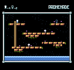
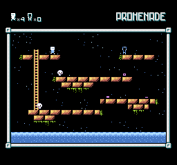