All-in-one dev cart for NES

This is an archive of a topic from NESdev BBS, taken in mid-October 2019 before a server upgrade.
View original topic
All-in-one dev cart for NES
by on (#78145)
Hey guys,

I've been working on a project lately that's similar to the PowerPak. Basically I love the idea of the PowerPak but really want to make my own for fun and as a learning experience. I would also like to make a portable NES at some point and then incorporate my hardware so I don't need to carry NES carts around in my pocket, which I hear doesn't work so well...

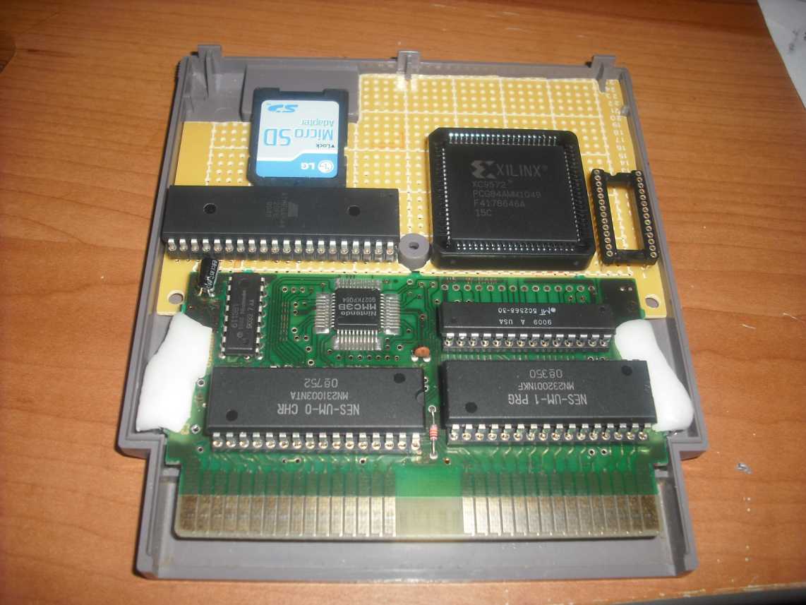
The main differences between my setup and the PowerPak is I'm using an Atmega664 and Xilinx CPLD vice a FPGA. I basically chose this because of I have experience with the two and none with FPGAs and NES programming. I almost went with a FPGA but I didn't want to figure out the configuration issues. Plus since I'm starting off with the actual MMC3 and MMC1 original chips really all I need my logic to do is MUX up the correct mapper's signal and recreate some of the basic CNROM/UNROM mappers etc. So my CPLD should suffice with nearly every pin spoken for, and I can always upgrade down the road.

I'm also going with SD micro vice CF, and programming my RAM chips with the atmega vice the NES like the powerpak does. Because of this I'm starting off with a external user interface to select the desired rom instead of an onscreen selection. I recognize on screen would be better but I don't have any NES programming experience yet. So that may be something I play with down the road.

To start off, I'm going to set my goal to allow all standard logic mappers (ie CN/UN/ANROM) and MMC1 and MMC3. This covers most of the games I own. Something I'd like to add is Tengen rambo1 for Rolling Thunder and MMC5 for StarTropics. But that wouldn't be until I have better idea what I'm working with and get a multilayer PCB made up so I can go surface mount for everything allowing more room to play with.

My IC lineup:
Atmega644 (may go the atmega1284)
Xlinix XCC-9572 CPLD
WRAM- 32K SRAM (thinner dip version)
PRG/CHR ROM/RAM- alliance 512KB SRAM as6c4008 (not pictured)
MMC3 (on SMB3 board)
MMC1 (to add on the right socket)
MUXs, counters, etc for programming the ROMs (not pictured to be added beneath the SMB3 board)

Anyways, Just thought I'd share my project with everyone. And open it up to comments, questions, and suggestions.
-Paul

Big image: MasterCart.jpg

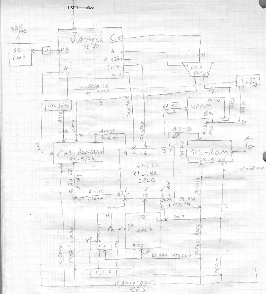
I don't really expect anyone to be able to read it but I've got my block diagram up too, if you're curious.
Big image: MasterCartBD.jpg
Priceless
by on (#78146)
There are some things money can't buy.
Image
For everything else there's MasterCart.

According to BootGod's NesCartDB, StarTropics is MMC6, which is MMC3 with different PRG RAM enable. You might be able to paper over the differences in your CPLD, or you might not. MMC5 is for Castlevania 3 and a bunch of Koei games.

by on (#78150)
HAHA that's awesome :) The powerpak was actually temporarily unavailable when I originally though up the idea, so there's more truth to that comment than one might think.

Yeah, sorry I had MMC5 on the brain from this morning. I meant MMC6. I haven't looked into MMC6 much but I did see a quick note that it was similar to MMC3. Once I get it up and working I wanted to look into it more. That would be cool if it was easy enough to just play around with the PRG RAM enable. Maybe I'll be able to play Star Tropics sooner than I thought!

by on (#78156)
I am VERY[/imfasis] interested in this project! I have all the NES programming skills you'll need for the project, just let me know what you want and what the hardware interface is.

I also have experience with AVR micro-controllers and can help you there if you need it.

I have looked into doing a project somewhat similar to this, but failed as I do not have enough hardware and CPLD knowledge.

I have already implemented MMC3 in Verilog, but you'd need the next larger CPLD family to fit it (or at least I did, I don't know much about this stuff).

Have you thought about using a larger CPLD for implementing all of the mappers, then using the JTAG port to reprogram the mapper code for every game? That's basically what the PowerPak does, but with an FPGA. You could cut down on burn-in problems by storing the current mapper number of the CPLD in the EEPROM of the AVR and only re-program the mapper CPLD when needed.

Anyhow, let me know what you need. I'll do anything I can to help out. Graphics, NES / AVR coding, heck I'll even code Verilog for you if you need it (test benches too), I'm just not terribly good with it :D

And if Microsoft will ever pay me for my dang game I can help pay for a prototype :x

by on (#78167)
WOW I didn't really think anyone would be interested in teaming up with me on this. I guess that's the beauty of open source though. So I'm curious what makes this project appealing? Is it just for fun? Or is there something better about it than the power pak? I don't own a power pak and don't know a whole lot about it beyond what the site advertises. My end goal isn't just to make a copy power pak but if there are things that the powerpak leaves to be desired I'm curious what. Is it because it's not open source? Does the addition of a microcontroller have significant benefits over the power pak?

Of course maybe your just like me qbradq in that you want to make something yourself.

It would be really cool if you were able to do NES programming to allow for an inscreen menu rom selection. I've taken an AVR assembly class and that's where my assembly knowledge stops. I might be able to use some help with AVR programming as well. Right now I'm trying to work out the SD card interface so I can program the ROMs and test out some basic mappers. Right now time is my biggest issue though, but hopefully that will change when classes get out in a month.

I'm taking a intro to VLSI class right now and and learning Verilog right now. But that's awesome that you've already got a working MMC3. I wanted to get the MMC1 and MMC3 integrated in with my logic instead of using the actual hardware, but this was the easy way for me to start. What do you require from a CPLD to pack the MMC3 into it? I knew it wouldn't fit in mine, and expected to upgrade to an FPGA whenever I moved from the MMC hardware. I basically got the biggest Xilinx CPLD I could that I could throw in a socket and stay through hole.

Quote:
Have you thought about using a larger CPLD for implementing all of the mappers, then using the JTAG port to reprogram the mapper code for every game? That's basically what the PowerPak does, but with an FPGA. You could cut down on burn-in problems by storing the current mapper number of the CPLD in the EEPROM of the AVR and only re-program the mapper CPLD when needed.


I think if we were going to go this route an FPGA is the answer. It solves both the logic capabilities and the any burnin issues. We would have to do something similar to the power pak if we went this route. I've found a project that uses SD card and MCU to configure the FPGA so we'd have to do similarly with our atemga.


You bring up a bunch of things that are a little farther down the pipeline than I was originally planning for the immediate future. But this is really because I was setting my immediate goals based on my skill set. I'd be willing to make some changes to my current design to incorporate some of these goals, I just want to take small steps making sure basic things go well before tackling bigger things like non-standard mappers.

The one major thing I would have figure out is how to interface the NES and atmega. I'm not really sure how this would work but here's what I'm imagining. The transistion between steps is what I'm really fuzzy on.

1) AVR boots and loads NES assembly and interface graphics to my PRG/CHR rams. Including the current list of available roms.

2) NES boots off that data and gives you the on screen rom selection menu.

3) User selects a rom and that gets communicated to the atmega somehow. Perhaps the NES writes to a specific location in WRAM or something? So the AVR would be waiting for a PRG /WR signal, and it would look at the value on the prg data bus. That number on the bus could then correlate to the rom number selected.

4) The AVR then needs to take control away from the NES so it can write the rom to PRG and CHR ram.

5) The NES starts to execute the game.

I'm thinking the only way to make steps 4 and 5 work is to hold the reset button on the NES console. So the NES isn't trying to execute garbage data and all kinds of bus conflicts while the atmega is writing to the ram chips. Is there a way to a software reset? Or handle this issue some other way?

I guess the power pak gets around this by having the NES program everything and then just points it's self to start executing the game. But this isn't really where I want to go with this.

I imagined getting around this whole issue by a using a hard user interface with the cart front with some push buttons and 7seg displays. You could just hold reset on the console since you're already at the console while everything was programming.

I'm not too concerned about money for a prototype. Really the hardware is pretty cheap. The multilayer PCB is what starts to get spendy. My controller conversion business brings in enough play money for me to splurge on stuff like this.

I kind of want to stick with through hole for right now, then once things are rolling and the hardware requirements are more clearly defined I could order up some more finalized boards and surface mount most everything.

And if there were people interested in it the project and wanted one themselves board cost would quickly become a non-issue. But I'm not really counting on this, I expected to just do everything myself and have everyone tell me I'm crazy for wasting all my time and money. And that I should have just bought a power pak:) But who knows.


If we really knew what we were doing it would be cool to incorporate a state saver and all other kinds of craziness. But that's not really a goal of mine. I'm not a big fan of "cheating" IMO if a game is too difficult to beat and I just keep trying over and over again great, you've consumed large amounts of my time that's that video games are for... It just gives an even bigger sense of accomplishment at the end.

by on (#78185)
The PRG ROM won't need to be taken off the bus while loading the game if the AVR talks to the SD card and feeds whole bytes to the NES, one at a time. Then the menu code copies the bytes to the RAM that implements PRG ROM, much as the PowerPak's menu reads bytes from the CF card's ATA interface. But the NES will have to pause for a moment while the AVR boots so that the menu can get loaded. Unless you have a (tiny) boot ROM in the cartridge, you'll have to somehow feed the NES a bunch of jog-in-place instructions.

by on (#78186)
infiniteneslives wrote:
WOW I didn't really think anyone would be interested in teaming up with me on this. I guess that's the beauty of open source though.


Yes, yes it is :D My project was also open source. I knew I lacked the hardware knowledge to get it to work and was hoping someone would pitch in :oops:

infiniteneslives wrote:
So I'm curious what makes this project appealing? Is it just for fun? Or is there something better about it than the power pak? I don't own a power pak and don't know a whole lot about it beyond what the site advertises. My end goal isn't just to make a copy power pak but if there are things that the powerpak leaves to be desired I'm curious what.


The PowerPak does not work on clone systems (like the Yobo for instance) and that is a deal breaker for me. Support for the clone systems is going to be very important to the future of the NES as a development platform. It's a major advantage we have over some of the other homebrew platforms.

Also using an SD card is a huge improvement.

infiniteneslives wrote:
Of course maybe your just like me qbradq in that you want to make something yourself.


I'd much rather by one off the shelf, but seeings as how none exist yet... :P

infiniteneslives wrote:
It would be really cool if you were able to do NES programming to allow for an inscreen menu rom selection. I've taken an AVR assembly class and that's where my assembly knowledge stops. I might be able to use some help with AVR programming as well. Right now I'm trying to work out the SD card interface so I can program the ROMs and test out some basic mappers. Right now time is my biggest issue though, but hopefully that will change when classes get out in a month.


Not a problem. There is plenty of code floating around the net, and even several FAT32 implementations we can use :D Remember, it's not reading the data off the drive that's the hard part, it's making sense of the file system that is challenging. I will slap a test bed together with my Arduino board and get to work on this.

infiniteneslives wrote:
What do you require from a CPLD to pack the MMC3 into it? I knew it wouldn't fit in mine, and expected to upgrade to an FPGA whenever I moved from the MMC hardware.


I ended up needing the 144 macro cell version, although I got the distinct impression that I was doing it wrong. Unfortunately I don't seem to have that code any more. I never uploaded it to SVN because I didn't want to "clutter the branch". That's usually a bad call :D

infiniteneslives wrote:
You bring up a bunch of things that are a little farther down the pipeline than I was originally planning for the immediate future. But this is really because I was setting my immediate goals based on my skill set. I'd be willing to make some changes to my current design to incorporate some of these goals, I just want to take small steps making sure basic things go well before tackling bigger things like non-standard mappers.


Small steps, got 'cha :D What you are proposing here would fill the need I am trying to get filled, so I am content with that.


infiniteneslives wrote:
1) AVR boots and loads NES assembly and interface graphics to my PRG/CHR rams. Including the current list of available roms.


The problem here is that the NES expects a reset vector to be available at CPU address $FFFC - $FFFD basically the instant you power up, and then the code that points to just a few clocks latter.

Seems to me the best way to address this is to include an 8KB (or 16 or 32) ROM on the board with the boot loader and menu system and have the power-on state of the board be to mirror all PRG reads to that 8KB ROM. Then this program would interface with the AVR to load program data into the RAMs, configure / set the mapper and turn control over to the program.

infiniteneslives wrote:
3) User selects a rom and that gets communicated to the atmega somehow. Perhaps the NES writes to a specific location in WRAM or something? So the AVR would be waiting for a PRG /WR signal, and it would look at the value on the prg data bus. That number on the bus could then correlate to the rom number selected.


Using an AVR to detect and react to the changing states of the address and data buses turns out to be a lot harder than it sounds, timing-wise. That's a tough problem really. Perhaps an 8-bit parallel to serial latch register on the data lines, with the latch line wired to R//W could be used.

infiniteneslives wrote:
4) The AVR then needs to take control away from the NES so it can write the rom to PRG and CHR ram.


The AVR taking control won't happen too easily, but here's one way that springs to mind:

1. Copy over the following routine from the boot loader into the NES's RAM
2. Executing from RAM, signal the AVR that it's safe to write to the CHR / PRG RAMs.
3. Wait for some signal from the AVR that it's time to execute the program (maybe an IRQ?).

infiniteneslives wrote:
I'm thinking the only way to make steps 4 and 5 work is to hold the reset button on the NES console. So the NES isn't trying to execute garbage data and all kinds of bus conflicts while the atmega is writing to the ram chips. Is there a way to a software reset? Or handle this issue some other way?


No software resets, sorry. The best we can do is jump to the restart routine to fake the program into thinking it is just powering up, but no way to effect the hardware itself.

You will either need to put a bus buffer on all PRG and CHR buses so you can disconnect them from the NES or you will need to allow the NES to program the PRG and CHR chips.

Now that we've talked it through, using the NES to program this chips probably is the best solution. We would have to have some way of passing data at high speed from the AVR to the boot loader, then have a command for the AVR to enable / disable the /WE lines of the RAMs.

infiniteneslives wrote:
I guess the power pak gets around this by having the NES program everything and then just points it's self to start executing the game. But this isn't really where I want to go with this.


Why? It seems to me to be the same thing, just one is doing everything on an AVR while the other has a (very small) routine on the NES to bang bits. And again if we run this routine out of system RAM we won't be stomping on ourselves or anything.

infiniteneslives wrote:
If we really knew what we were doing it would be cool to incorporate a state saver and all other kinds of craziness. But that's not really a goal of mine. I'm not a big fan of "cheating" IMO if a game is too difficult to beat and I just keep trying over and over again great, you've consumed large amounts of my time that's that video games are for... It just gives an even bigger sense of accomplishment at the end.


I agree with that. State saving requires direct access to the hardware, something we won't have. All we see is a slice of the buses. Now retaining and reloading SRAM is a must, otherwise games like Zelda and Final Fantasy will not be very playable.

That introduces more issues. Storing the data is easy, just write it to the SD card with some kind of hash value or long file name. As for restoring that data that's a no-brainier too, just load it the same way you do everything else.

The hard part is when and how to read the SRAM. One solution that springs to mind is this:

1. Provide a conventional battery-backup circuit for the SRAM.
2. Store what game you have loaded in the EEPROM of the AVR.
3. At power-up, read the game info from the AVR to determine if we need to back up the SRAM from last time.
4. If so, read the SRAM and feed it back to the AVR for saving to the SD card.

One thing you might want to keep in mind is that may games use RAM instead of ROM for their CHR memory. You will need to understand that the /OE and /WE lines of your CHR-RAM will need to be attached to the CHR bus as well. I couldn't tell from your block diagram if you had taken that into account.

by on (#78195)
My bad, was pointing to the all-in-one console. Sorry for my stupidity. But yeah the powerpak is there, but still I wouldn't hesitate to do it if I were you. Seems like a great challenging project! There's the Tototek SNES flash cart and the Super PowerPak. Doesn't seem like a bad thing for more tech to be made especially if you have fun with it! Good luck. :)

by on (#78197)
@3gengames
I think they are talking about a PowerPak like development cart and not a new NES clone or something.
Maybe I misunderstood your post, but it seems to me like you misunderstood this thread due to a misleading title that fooled me before.


[Good point. Preposition added. --MOD]

by on (#78202)
Quote:
Using an AVR to detect and react to the changing states of the address and data buses turns out to be a lot harder than it sounds, timing-wise. That's a tough problem really. Perhaps an 8-bit parallel to serial latch register on the data lines, with the latch line wired to R//W could be used.


Correct me if I'm wrong. I agree you latch idea would work, but if we were running at 20Mhz wouldn't we have around 10 clock cycles to catch the bus's data?

A thought: Doesn't the cart have a 21Mhz clock available to it? Is that just an undivided clock that the CPU is running off of? What if we drove our atmega off that clock? Would that help out with timing issues? Could we watch the bus and then sync up with the CPU? Let me know if I'm crazy.


Quote:
Not a problem. There is plenty of code floating around the net, and even several FAT32 implementations we can use Very Happy Remember, it's not reading the data off the drive that's the hard part, it's making sense of the file system that is challenging. I will slap a test bed together with my Arduino board and get to work on this.


I've been going off this guy's work:http://frank.circleofcurrent.com/cache/fat_sd.htm got stuck somewhere with something doubly defined or something and couldn't find where I was doing it... I need to sit back down with it.


Quote:
You will either need to put a bus buffer on all PRG and CHR buses so you can disconnect them from the NES or you will need to allow the NES to program the PRG and CHR chips.

Now that we've talked it through, using the NES to program this chips probably is the best solution. We would have to have some way of passing data at high speed from the AVR to the boot loader, then have a command for the AVR to enable / disable the /WE lines of the RAMs.


Yeah when you spell it out like that I agree. The 30 buffers might be okay on surface mount but not with what I've got now. I guess we're trading sitting on our ass for the 30 sec it takes to program for getting up and hitting reset for a few seconds it would take for the AVR to program it. Now that I think about it the avr won't be 10x faster because it's getting the data from the SD card serially. So the time difference is negligible 25 seconds vice 30... I'd rather sit on my ass and take a beer break.


Quote:
The hard part is when and how to read the SRAM. One solution that springs to mind is this:

1. Provide a conventional battery-backup circuit for the SRAM.
2. Store what game you have loaded in the EEPROM of the AVR.
3. At power-up, read the game info from the AVR to determine if we need to back up the SRAM from last time.
4. If so, read the SRAM and feed it back to the AVR for saving to the SD card.

One thing you might want to keep in mind is that may games use RAM instead of ROM for their CHR memory. You will need to understand that the /OE and /WE lines of your CHR-RAM will need to be attached to the CHR bus as well. I couldn't tell from your block diagram if you had taken that into account.


Yeah I was kind of delaying the game save for after things were working well. I would like to have a plan though atleast for now to save the WRAM save data.

I think the power pak does this when coming out of reset after you've played a game you want to save. Which seems logical. Couldn't we just have that as a menu option? We could even take note that we just came out of reset from a savable game and prompt the user to save? And if there weren't battery data just go back to the menu?

So we would just copy the SRAM to the SD card and move on. And not have to bother with saving it to EEPROM and comparing and everything?

Yeah I do understand about the CHR-RAM/ROM. I know it needs to be handled, I just didn't include it.

Quote:
The PRG ROM won't need to be taken off the bus while loading the game if the AVR talks to the SD card and feeds whole bytes to the NES, one at a time. Then the menu code copies the bytes to the RAM that implements PRG ROM, much as the PowerPak's menu reads bytes from the CF card's ATA interface. But the NES will have to pause for a moment while the AVR boots so that the menu can get loaded. Unless you have a (tiny) boot ROM in the cartridge, you'll have to somehow feed the NES a bunch of jog-in-place instructions.


Quote:
The problem here is that the NES expects a reset vector to be available at CPU address $FFFC - $FFFD basically the instant you power up, and then the code that points to just a few clocks latter.

Seems to me the best way to address this is to include an 8KB (or 16 or 32) ROM on the board with the boot loader and menu system and have the power-on state of the board be to mirror all PRG reads to that 8KB ROM. Then this program would interface with the AVR to load program data into the RAMs, configure / set the mapper and turn control over to the program.


This is what I was most concerned about... I want to try to figure out how we're going to do this with the hardware as the first priority. We need to clearly define the interface between the NES and AVR.

The issue is communicating the selected rom , save data, and menu navigation.

I like the idea of a small chunk of memory I'd like to go with SRAM and either battery back it or we could require the user to hold the reset button at console power up and then load the boot menu and everything we needed to it. I'm kinda thinking it would be nice if it were dual ported, but I'm not sure.

So then instead of Prg /CE enabling our PRG-ROM we'd have it enable our "BOOT-RAM". I'd like it to be as small as possible like 8K. Now that I think about it though... I've already replaced my 8K of WRAM with 32KB SRAM. What if we just put our boot menu in the upper 24-16K of my WRAM? And make it appear to be $FFFC - $FFFD to the NES. We'd have to control all this with logic and the AVR.

We'd still be requiring the user to hold reset durring the initial power up, so we could load our boot menu, but that's it. And still use the lower 8K of my WRAM for it's original purpose.

Just brain storming here. I'm all ears for ideas and pointing out where my knowledge is flawed.

P.S. you guys will have to let me know how I can make the user name show up in my quotes. I couldn't find anything in the FAQ.

by on (#78204)
Thinking about my idea of using the memory I already have still has the issue with the AVR accessing it so things can be communicated back and forth...

Perhaps if my "WRAM/BOOTRAM" were dual ported???

If this sounds like a good solution to ya'll I'm interested in what your suggestions are for specific part numbers.

Here's what I'm thinking:

-16K minimum, could be 8K if separated from the WRAM and have the NES copy and load our save data too.
-asynchronous
-dual ported
-through hole or J-lead package that's socket-able. Something that can be easily prototyped now, but be moved to a surface mount package with the final layout. This isn't a firm requirement, I could easily make a surfboard for it if it were a coarser surface mount part, but this would be preferred.

I'm not finding a lot that meets this though. So that may trash this idea...

by on (#78205)
I made a cart that is somewhat like this, about 6 or 7 years ago. I used a PIC18 because it had a parallel port peripheral, which made communication with the NES dead simple. I don't know if the AVR has something similar, I never used one but I guess not. Mistake I made in the first version was not putting the RS232 transceiver on board, instead there was a 6-pin header with TTL-level serial on it because I figured that would allow interface boards for RS232, MIDI, or an SD card. But I only got as far as doing RS232 with it, and having that on a separate board just made it more of a pain to build. Now it's also easier to get an MCU that has 3 more UARTs on it, no need to share the same one for everything.

I don't think you'll be able to use the 21Mhz clock. I don't know what the clock signal looks like exactly, but I do know that absolutely nothing ever used it, and it was dropped entirely from the top-loading NES. So I doubt it would be on any clones (and it's definitely not on Famicom or Famiclones).

My board used just a few 74HCxx parts for the mapper, I didn't know how to use a CPLD at the time. Sometime (before too long I hope) I'm going to redesign the board to work in a much smarter, and extremely more powerful setup. I guess the big difference with the mappers I've been coming up with is that I never gave a crap about it being compatible with Nintendo's ASIC mappers. Since I figured it's optimized for writing new stuff, where using the old ASIC mappers are more of a hindrance than anything. A big focus on my mapper wasn't just using the PIC to handle boring system tasks, but to use it more like a coprocessor for the NES. It was really successful at it, I got 4 channels of wavetable sound out of it, and had it able to handle lots of other stuff at the same time.

Yeah, for dual-ported RAM I don't think there is anything appropriate to use. For my redesign I've wanted that, and I've settled on using a fast synchronous SRAM and making a homemade memory controller for it.

by on (#78207)
Quote:
I used a PIC18 because it had a parallel port peripheral, which made communication with the NES dead simple. I don't know if the AVR has something similar, I never used one but I guess not.


What do you mean by parallel port peripheral? I'm missing something here...

by on (#78208)
infiniteneslives wrote:
A thought: Doesn't the cart have a 21Mhz clock available to it?

NTSC NES has the undivided 21.5 MHz clock. PAL NES has the undivided 26.6 MHz clock (I think). Famicom has no undivided clock.

Quote:
We could even take note that we just came out of reset from a savable game and prompt the user to save? And if there weren't battery data just go back to the menu?

This is exactly what the PowerPak does, based on the battery bit.

Quote:
The issue is communicating the selected rom , save data, and menu navigation.

It might be possible to do all the FAT work on the 6502, as the PowerPak does, and consign the AVR to just reading and writing SD sectors.

Quote:
So then instead of Prg /CE enabling our PRG-ROM we'd have it enable our "BOOT-RAM".

Ever heard of something called a "suicide battery"?

Quote:
I've already replaced my 8K of WRAM with 32KB SRAM. What if we just put our boot menu in the upper 24-16K of my WRAM?

Then 1. the three SXROM games (PR8 and two Japan-only RPGs) that use all 32 KB would interfere with the boot menu, and 2. loss of battery power would render the cart inoperable.

Quote:
We'd still be requiring the user to hold reset durring the initial power up

That could be a pain and lead to tech support calls and even product returns from people who don't RTFM. What's the cost of this support, compared to the cost of, say, a 2 KiB ROM chip that can load the full menu (mcart.ipl) from the root directory?

Quote:
P.S. you guys will have to let me know how I can make the user name show up in my quotes. I couldn't find anything in the FAQ.

You can click the "quote" button at the top right of a post, which inserts the BBCode syntax [quote="tepples"]...[/quote].

by on (#78212)
tepples wrote:
NTSC NES has the undivided 21.5 MHz clock. PAL NES has the undivided 26.6 MHz clock (I think). Famicom has no undivided clock.


I'm ready to ditch the thought of using the cart's clock.

Quote:
Ever heard of something called a "suicide battery"?

Quote:
I've already replaced my 8K of WRAM with 32KB SRAM. What if we just put our boot menu in the upper 24-16K of my WRAM?

Then 1. the three SXROM games (PR8 and two Japan-only RPGs) that use all 32 KB would interfere with the boot menu, and 2. loss of battery power would render the cart inoperable.

Quote:
We'd still be requiring the user to hold reset durring the initial power up

That could be a pain and lead to tech support calls and even product returns from people who don't RTFM. What's the cost of this support, compared to the cost of, say, a 2 KiB ROM chip that can load the full menu (mcart.ipl) from the root directory?


Some of these issues are of non-concern to me right now. I didn't really plan on selling these and providing support for them. Not to say that I'll never consider it though.

Battery backed ram is a good option for what I'm already working with. I'll just fix it myself if I kill the battery. Or, just do without the battery and have the AVR load it up while the user is holding reset during power up. (although I'm not certain this will work)

I also don't care much about SXROM games right now like I said before I want to get the basic logic mappers and MMC1 and MMC3 in their more common board configurations. If this whole project became really refined though I agree with the use of a 2KiB rom chip in a final draft type stage. This would be a simple upgrade from the hardware already used by the prototype.

I like all of these points though, and it's best to think about how it could be made better and allow for simple improvements to be made in the future that would add the capabilities people might be looking for. Right now I'm heavily limited by the fact I'm sticking to through hole components. But I'd rather find out what works and what doesn't on something that's easy to modify. I don't want to drop significant money on a multilayer PCB that ends up being a rough and drafty design that's difficult to modify. I can't do as much with surface mount components and hidden wire runs.

I'm going to lean on the simplest options now, and take notes as I go on how I want to improve it for the next draft.

by on (#78217)
infiniteneslives wrote:
Quote:
I used a PIC18 because it had a parallel port peripheral, which made communication with the NES dead simple. I don't know if the AVR has something similar, I never used one but I guess not.


What do you mean by parallel port peripheral? I'm missing something here...


I mean the PIC directly used /CE, /RD, /WR, and the NES CPU data bus. I used the mode described in this doc.

by on (#78226)
Memblers wrote:
infiniteneslives wrote:
Quote:
I used a PIC18 because it had a parallel port peripheral, which made communication with the NES dead simple. I don't know if the AVR has something similar, I never used one but I guess not.


What do you mean by parallel port peripheral? I'm missing something here...


I mean the PIC directly used /CE, /RD, /WR, and the NES CPU data bus. I used the mode described in this doc.


Oh I get it. It basically allows the NES to write to the mcu's port as a parallel latch, that is pretty nifty...

So did you just drive the /WR input on you pic with PRG /WR ? I guess that's pretty much the same type of setup qbradq was talking about except we would need an external latch/regisiter for the NES to write to.

I guess if we only had a few things the NES needed to communicate to the AVR (not the other way) We could have one PISO shift register for everything. Then the AVR could just read from the Shft reg and decode whatever "opcode" we create.

That would allow us to tell the AVR we needed to navigate around the directories, and load roms, save battery backed RAM and what not. It could either be packed in the CPLD or an external chip for now since how I'm running out of pins.

It's becoming apparent I need to dig deeper into the NES architecture and opcodes though, now that the scope has been changed to a user onscreen rom selection.

The part I need to understand before I can build anything is how the atmega will feed bytes to the NES that in turn get programmed to both CHR and PRG ROMs.

I guess I'm imagining a second data register that the AVR writes to. And the NES reads from and then writes that byte to the correct byte in PRG/CHR ROMs.

Sounds simple, but I'm struggling with how to set everything up in the cart for the NES to do all this.

I'm assuming based on an earlier comment that we can put these read write instructions over to the NES's RAM that way the boot menu no longer needs to be accessed. I'm also assuming their is an opcode to load this into a internal register in the NES. And the NES has a (X,Y,Z) or some sort of address pointer register that we can keep incrementing. Hopefully there is a store with post-increment of this address pointer...

So a byte could be copyed from the data buffer to the ROMs in two clock cycles as follows:

1) Then the cartridge could be set up so all PRG R/W read signals would enable data register regardless of the address bus (or not? perhaps we require PRG /CE and a specific Address bit to be high also?).

2) The cart would be setup up so it can write to PRG/CHR ROMs like it would normally. (ie, PRG(CHR) R/W, /CE and address busses are aligned to the roms) Now the NES writes the byte to the address pointed to by the (X,Y,Z?) register and Post-increments that register.

Once the PRG ROM was programmed the NES would have to count itself to know were done, it would now start programming the CHR ROM if applicable. I'm also not sure how this all goes down with the CPU and PPU. Would we want to have a separate PRG and CHR data register for the CPU and PPU to copy from? Or is it better to just let the CPU load up the "CHR-ROM" in a similar manner to however it works with games that use CHR-RAM like AOROMs? Is there some way to speed up the process and have both the CPU and PPU filling their respective ROMs in tandem? Assuming the AVR is keeping up with the process?

We could also make things easy for the NES by "turning the pages" of the PRG and CHR ROMs. Basically just keep track of where we are in the "page" and send a signal from the AVR to the CPLD to change the upper unaddressable address bits. That way we wouldn't have to create our own mapper for the NES, and could just have the address counter roll over with each page.

I'm not sure how all this works for the NES as I said before, but if needed could we just give the NES and infinite loop to copy everything over and send and IRQ? So the NES would know we're done and just point it to start executing the game.

If someone wants to take the time to fill in my knowledge holes here great, otherwise I'm perfectly capable of doing the research myself just send me on my way. I just imagine that my assumptions are fairly close to reality.

by on (#78256)
I'm not sure if you mean have the NES do the memory writing (surely then the communication would need to go both ways), or to have the circuit on the cart write to memory while the NES "isn't looking".

The latter method would work well, it could be fast but needs all the bus buffers on board (and double it all for handling CHR the same way). It would work similar to a ROM emulator, but the NES would disable NMIs and IRQs and run inside the internal RAM during loading. BTW, that ROM emulator would make any cart into a devcart, if you want an easy solution. :P

I think having the NES communicate with the MCU is a lot more interesting. Mostly because if the hardware is there, might as well let the NES itself use it. The communication with the PIC on my Squeedo cart seemed kinda complex, with the NES interrupting the PIC, and the PIC interrupting the NES, but it seemed decently fast. PIC32 has an even nicer parallel port, it added a 4-byte FIFO buffer (or alternatively, 2 address inputs). That's enough memory for the NES execute an instruction + RTS out of it.

I have a pretty extreme NES cart project pretty much entirely planned out, just don't have the time to work on it much until I finish other projects. But it'd be using an FPGA, PIC32, and other fun stuff. Only part ready now is some of the PIC32 code (in C). The main trick will be doing the memory controller, like I mentioned earlier I'm wanting to use a synchronous RAM and I'd be running it really fast, up to 100mhz if needed. There's been a lot of mentions about open-sourcing hardware, I've considered doing something like that. But I'm not sure if it would help much before the board is made yet. Most of the stuff to get working will be in the Verilog and coding the PIC32.

by on (#79372)
Hello, NESdev community!

Several days ago me and my friend played some games on his NES clone. He don't have any cartridges, except, built-in 361 (or so) in 1. There were some fun games, but most of them were spoiled by bad trainers. For example we didn't know what we supposed to do in Devil World, until I went to GameFAQs and found that there are supposed to be dots to collect, which hadn't appeared, at least I couldn't found a "pure" menu item for this game (without some trainer suffix).

So after some hours of nostalgia we decided we need some new cartridges. I have some Chinese multicarts (we don't have any legal NES games in Russia thanks to Nintendo marketing strategy), so after some more thinking we came up with idea of obtaining a reprogrammable cartridge to play some genuine ROMs.

I've googled some finished projects to assemble and found that most of them are commercial, except NESFunkyFlashCart, but it is so obscure (I've barely found a mirror of it's homepage at some Russian site) that I didn't even want to look deep into it's schematics. It also loads games too long (10 minutes for 512K).

We both are studying at university as hardware engineers, so we know how to design (well, more or less) electronic circuits and we thought that we can invent something new and maybe sell it in case of success. So I've started to search and read NES docs. After a couple of days googling and reading I found that forum topic. As I understood, nesinfinitelives are working on quite similar project (what a lucky finding) and I think we can help each other.

ATM I came up with following scheme: the cartridge will have two SRAM chips to hold the game's data and an ATMega MCU (I've been studying them for the last half of the year) to load them through UART and behave as a mapper. I decided to start with something simple like UNROM and Contra/Duck Tales. We don't want to use PLDs, because they aren't cheap (almost same price as everything I've listed here) and we don't have much experience using them.

I have understood most of the NES' architecture but there are some questions left:

1) Somewhere I found a statement that using an MCU alone would be too slow, because there aren't much time left to decode address and fetch data from ROM/RAM. Is it true? How does data fetching from cartridge work? Let's imagine we have the following code (I haven't learned 6502 ASM yet, so I will use textual descriptions):
Code:
1: Set memory address
2: Load the data

At which point of time the data will be loaded in CPU: after the second command or in the middle of it? How much time (estimated) is left for mapper to decode an address? Also am I right that every 6502 instruction needs only 1 cycle to execute?

2) What does NES' CPU do after power on?

3) Someone said at the first page that it is impossible to reset the NES from cartridge. What does the /IRQ pin in cartridge slot does then?

Looking for your answers. Thanks in advance.

by on (#79373)
NES takes a few cycls per instruction, I think it's like 2-5 or something like that. I don't think any instructions take 1 clock.

The PIC/AVR as a memory mapper has been thought about I am pretty sure and nobody thinks it is plausible to build a mapper that does anything special at all, because the only thing it can really do is logic and that's cheaper than a micro controller anyway.

And then there's this, and this site:

http://www.retrousb.com/index.php?cPath=24

http://www.retrousb.com/index.php?osCsi ... 831304a006

Also, IRQ means interrupt.

by on (#79377)
Yeah the only mappers I could see easily replicated with a MCU are ones that use the 74ls161 and 74ls32 or similar. But I think your limiting factor with using a MCU is i/o, these mappers suck up pins quickly if you're trying to implement several of them. You'll have a hard time sticking to through hole options.

So check into the AOROM, UNROM, CNROM, etc. and of course you could do NROM.

When working on these carts myself I found a lot talking about how these mappers worked from a software standpoint but little to none explaining the circuity (no schematics). Consequently I've traced out all the runs on those carts and have some rough schematics of my own, but I'm not sure if anyone could read them. :) But I would like to get them posted up at some time in the future.

If you want to replicate the MMC1 and MMC3 etc you'd have to look into programmable logic. Even with this layout I have in this post I planned to use the actual hardware. It's conceivable to get away with using a MASSIVE mcu on the other end instead of the CPLD I was. But I doubt that'll be cheaper or easier than my $7 CPLD. Plus you would have to look into surface mount and with my prototype here I wanted to stay through hole.

If you're looking for an easy way to handle the reset and loading SRAM issue I recommend holding the reset button or having a separate power supply for your cart so you could program it before inserting the cartridge. That was my plan here, I know it's not elegant but it's easier in my mind at least.

by on (#79384)
You have (1 / 1789772.72727272) / 2 = 279 ns before your hold conditions to decode writes. For reads you will have less time to satisfy the hold condition of the CPU, which being old is significant. To be safe you should decode and provide valid data within 200 ns (same with the PPU if you implement CHR ROM stuff). Logic mappers get away with 200 ns *ROMs* because the mapper's output address lines track the CPU's input address lines which are settled BEFORE the start of Phi2. You won't have that luxury.

You'll have to interrupt on the rising edge of Phi2, sample R/W and the address and decode. For writes data is valid and must be sampled at the falling edge of Phi2. For reads decode as fast as possible but put the bus back to Hi-Z on the falling edge of Phi2.

That's pretty much all there is to it, but good luck with that lol I think you'll need a very high performance (100+ MIPS) MCU. There's some Atari cart which uses a really fast MCU exactly this way, but then again the largest Atari games are <= 32k so they can fit in a MCU's flash/RAM, they have extremely basic bankswitching with little to no combinatorial logic after a register, and the CPU is 70% slower.

by on (#79386)
Thank you for such fast replies!

3gengames wrote:
NES takes a few cycls per instruction, I think it's like 2-5 or something like that. I don't think any instructions take 1 clock.

The PIC/AVR as a memory mapper has been thought about I am pretty sure and nobody thinks it is plausible to build a mapper that does anything special at all, because the only thing it can really do is logic and that's cheaper than a micro controller anyway.

And then there's this, and this site:

http://www.retrousb.com/index.php?cPath=24

http://www.retrousb.com/index.php?osCsi ... 831304a006

Also, IRQ means interrupt.


Thank you for links, but I know about PowerPack already. Considering /IRQ pin I think it is possible to "hang" NES in infinite loop somewhere (cheap small SRAM, for example) during game load, then send an /IRQ which should set PC to 0, while MCU is switching NES to SRAM with game.

Quote:
When working on these carts myself I found a lot talking about how these mappers worked from a software standpoint but little to none explaining the circuity (no schematics).


I have exactly same problem: can't really understand UNROM schematics from wiki for example. How it is suppossed to make last bank always visible with an OR gate connected like that? Well, i don't quite understand how it is connected... :D

Quote:
If you're looking for an easy way to handle the reset and loading SRAM issue I recommend holding the reset button or having a separate power supply for your cart so you could program it before inserting the cartridge. That was my plan here, I know it's not elegant but it's easier in my mind at least.


Here is my current idea (untill I implement my /IRQ-based algorithm):
-Plug the cartridge into a NES(clone).
-Connect the cartridge to PC to power it and load a game.
-Turn on NES.
-???
-Profit!

Too bad I'm passing exams ATM so I can't work much on my device, but I really hope to finish some prototype until next month.

Quote:
You have (1 / 1789772.72727272) / 2 = 279 ns before your hold conditions to decode writes. For reads you will have less time to satisfy the hold condition of the CPU, which being old is significant. To be safe you should decode and provide valid data within 200 ns (same with the PPU if you implement CHR ROM stuff). Logic mappers get away with 200 ns *ROMs* because the mapper's output address lines track the CPU's input address lines which are settled BEFORE the start of Phi2. You won't have that luxury.

You'll have to interrupt on the rising edge of Phi2, sample R/W and the address and decode. For writes data is valid and must be sampled at the falling edge of Phi2. For reads decode as fast as possible but put the bus back to Hi-Z on the falling edge of Phi2.

That's pretty much all there is to it, but good luck with that lol I think you'll need a very high performance (100+ MIPS) MCU. There's some Atari cart which uses a really fast MCU exactly this way, but then again the largest Atari games are <= 32k so they can fit in a MCU's flash/RAM, they have extremely basic bankswitching with little to no combinatorial logic after a register, and the CPU is 70% slower.


That's a very useful information, but how you calculated those 279ns? 2 cycles per instruction? And where that Phi2 came from? Datasheet?

by on (#79387)
I don't really think there is much room to make profit here. The powerpak pretty much has everything covered and most people have one already that would consider buying what you're selling. You're NOT going to get anywhere's close to as capable as the powerpak with just an MCU and leaving out programmable logic.

I would use this as more of a learning tool or project for fun kinda like what I'm doing. But it's really your decision, ignoring me could make you money in some way I'm not seeing.

If you PM me with your email I can send you my hand drawn schematics and you can attempt to decipher them. I deem them too ugly to post. But really it's pretty simple the 161 acts as a latch not the counter it is. Then the or gates just make it so the last page is always visible. A schematic makes this a lot easier to see.

by on (#79388)
Duck_tech wrote:
I have exactly same problem: can't really understand UNROM schematics from wiki for example. How it is suppossed to make last bank always visible with an OR gate connected like that? Well, i don't quite understand how it is connected... :D

When accessing $8000-$BFFF, PRG A14 is low, when accessing $C000-$FFFF, it's high. If you OR A14 with the bank index, the result will always be all 1's when accessing $C000-$FFFF. That's how the last bank gets hardwired to the top half of the addressing space.

by on (#79389)
Duck_tech wrote:
I have exactly same problem: can't really understand UNROM schematics from wiki for example. How it is suppossed to make last bank always visible with an OR gate connected like that?

Address line A14 can have a low (0) or high (1) logic level. It's low when the CPU address is in $8000-$BFFF and high when the CPU address is in $C000-$FFFF. If you take four copies of A14 and make a binary number out of them, you get 0000 (when $8000-$BFFF) or 1111 (when $C000-$FFFF). ORing the bank number with 0000 gives you back the same bank number, but ORing the bank number with 1111 produces 1111, which means the last bank in the cart.

(I got ninja'd by tokumaru.)

Quote:
Here is my current idea (untill I implement my /IRQ-based algorithm):
-Plug the cartridge into a NES(clone).
-Connect the cartridge to PC to power it and load a game.
-Turn on NES.

So if I understand you right, the cartridge is programmed while sitting in the NES Control Deck and a cable is coming out the Game Pak slot. Mostly I worry about the effect of putting voltages on the cart edge pins while the NES is powered off. Can anyone else comment about this?

Quote:
That's a very useful information, but how you calculated those 279ns?

The clock period is 315/176 MHz, or about 1.79 MHz. This means each clock period is 176/315 * 1000 ns, or about 558 ns, and the half period is 279 ns.

Quote:
2 cycles per instruction?

The 6502 reads or writes a byte of memory during every cycle, and the memory has to be fast enough for this. A 2-cycle instruction will read the opcode in the first cycle and the operand in the second.

Quote:
And where that Phi2 came from? Datasheet?

Phi2 is the CPU's clock signal. It comes from a circuit in the CPU that divides the master oscillator by 12 (NTSC), 16 (PAL NES), or 15 (some PAL famiclones).

by on (#79390)
Duck_tech wrote:
That's a very useful information, but how you calculated those 279ns? 2 cycles per instruction? And where that Phi2 came from? Datasheet?
Yes look at a 6502 datasheet. Phi2 is the clock phase where external data is accessed.

279 ns is half of ONE clock cycle. That's how fast you must provide data to the 6502... Unlike other synchronous-microcoded processors the 6502 accesses the bus every cycle of every instruction.

For reads it's absolutely necessary to decode a write to memory and get data to the CPU within 279 ns when Phi2 is over (and Phi1 begins).

For writes (PRG bankswitching) you must capture the write after 279 ns, but the soonest the CPU can access this data again is near the end of the next Phi2 so you basically have 1.75 clock cycles to process a write (actually ~50 ns less because you have to wait for the /ROMSEL signal to be decoded inside the NES) and process a read. Let's call it 1.5, so you might have 800 ns for a write then a read/another write, or 200 ns per read (maybe a little more if you start decoding before Phi2 but it's tricky because you can't be sure the address bus has settled until Phi2 and you'll still have to wait for the NES's internal address decoding).

I was wrong about the Atari's speed too, it's ~1.19 MHz so it's 50% slower. The Harmony Cart runs at 70 MHz = 70 MIPS? though so you'll probably need 140+ lol.

by on (#79414)
tepples wrote:
Quote:
Here is my current idea (untill I implement my /IRQ-based algorithm):
-Plug the cartridge into a NES(clone).
-Connect the cartridge to PC to power it and load a game.
-Turn on NES.

So if I understand you right, the cartridge is programmed while sitting in the NES Control Deck and a cable is coming out the Game Pak slot. Mostly I worry about the effect of putting voltages on the cart edge pins while the NES is powered off. Can anyone else comment about this?


I'm not sure but I think most everything is powered off that same 5V bus so you'd end up trying to power up the NES with your USB cable.

One way to get around this would be to auctioneer the power from the two supplies with some diodes. But I still don't know if all that is the best idea...