As a lunchtime and after-work activity, I have slowly built and finally completed a setup to hack the MMC5.
- 8x 16-bit TTL-compatible I2C I/O expanders (totaling 128 bits I/O)
- USB to I2C adapter
- Donor MMC5A chip from 'Just Breed', removed successfully
- 0.65mm pitch QFP-100 20x30 breakout board, MMC5A mounted on it successfully
- All connections from I/O expanders to MMC5 complete (except audio)
- Preliminary C# GUI on computer to create automated tests, to let it run overnight, etc.
Attachment:
File comment: MMC5 hack rat's nest
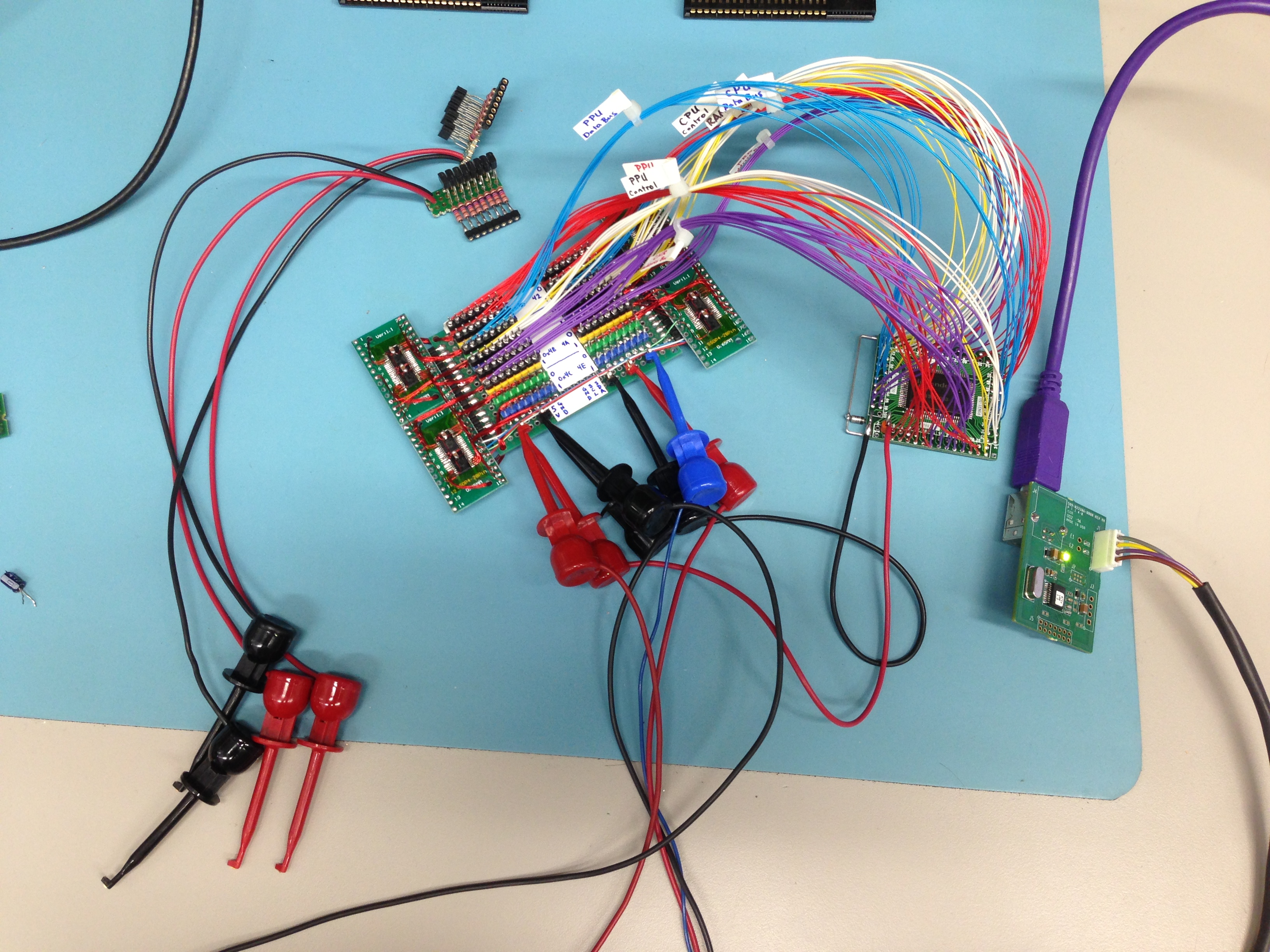 IMG_1541.JPG [ 2.4 MiB | Viewed 22174 times ]
I put a series 100 ohm on each pin in case I goof up and hook 2 outputs together, hopefully saving it if that happens. I have a current-limited voltage source I plan to use as well. The I/O expanders default to input when power is applied and have a 100k internal pull-up when set as input. I created controllable 10k pull-downs for the CPU and PPU data busses so I can test whether the MMC5 is driving the bus or is in open bus / high impedance state.
The first auto-test that I want to create is to try reading from all possible CPU addresses, recording whether the MMC5 is open bus or reporting a value. If it is a value, recording the value. This will tell us each and every address to which the MMC5A responds, and nail down that aspect for the memory map. I will get this test working first, then we can think about what to do next. I would like to start reading and writing to PRG-RAM and watching the unknown lines in the not-too-distant future. I am pretty sure we will be OK on noise and wire length because I will be controlling the M2 line manually with the I/O expanders. This will definitely be a very slow-mo test process.
My goal is to work on the GUI this weekend and see if I can get some sort of test running. Will report progress!
Ben Boldt wrote:
The first auto-test that I want to create is to try reading from all possible CPU addresses, recording whether the MMC5 is open bus or reporting a value. If it is a value, recording the value. This will tell us each and every address to which the MMC5A responds, and nail down that aspect for the memory map.
I believe this test was done many years ago using a CopyNES, and it revealed that the only readable addresses were $5010, $5015, $5204-$5206, and $5C00-$5FFF
if ExRAM is in "ordinary RAM" mode (i.e. last value written to $5104 was 2 or 3).
Still, it never hurts to recheck these sorts of things, and it'll still be useful in confirming that your testing rig is working correctly.
Here is what I found today:
With these settings:
CPU R/W = 1
/ROMSEL = 1
M2 = 1
The MMC5A drives the CPU data bus when reading from these addresses:
$5010: $01
$5015: $00
$5204: $00
$5205: $01
$5206: $FE
$5208: $C0
$5209: $00
$5C00 - 5FFF: all $00
All reads result in open bus when /ROMSEL = 0.
When M2 = 1, MMC5 register data appears on CPU data bus asynchronously. For the entire test, I stuck M2 = 1, no toggling. However, running my same test with M2 = 0, the data bus is always open bus. I would suspect that the data bus updates when M2 = 1 and then latches whatever it had when M2 = 0.
Interesting to consider what the heck $5208 and $5209 are doing. This comes right after the 8x8->16 multiplier.
Ben Boldt wrote:
However, running my same test with M2 = 0, the data bus is always open bus.
Isn't that what you expected? What were you testing for?
Quote:
I would suspect that the data bus updates when M2 = 1 and then latches whatever it had when M2 = 0.
I fully expect it's the "normal" transparent latch interface we've seen through the design on the 2A03 / 2C02...
I want you guys to know that I am going to be pretty new to a lot of this -- I have done a few things where I have changed ROMs in cartridges, but I have never gone deep like this. Never before have I had a need to think about which edge of the clock the data bus is updated, etc, so this is going to be pretty awesome for me, and maybe a little elementary for some of you veterans. I am good at making fancy tools and stuff to help me explore and learn, that is my forte. I would like your ideas to help design more useful tests. I do have all pins controllable with this setup, except for audio.
Anyway, I think that this test has proven that my tools are running pretty well. I might try messing with the multiplier next, seeing how many clocks it requires (if any) to get the correct result. Then I might poke at 5208/5209. Does anyone have any idea what these 2 registers might do? Hopefully it is a divide, that would be awesome.
Ben Boldt wrote:
I want you guys to know that I am going to be pretty new to a lot of this
Ah, ok. That makes sense!
My best guess is that $5208 and $5209 expose some portion of the internal multiplier state.
The only real thing left to be done with the MMC5 audio is characterize its amplifier. The last time I hooked up this copy of Laser Invasion to anything I apparently only got as far as measuring its slew rate: the really quite slow 0.42V/µs. But I never got as far measuring a transfer curve ... ok, fine, I should stop putting that off...
I hooked up a variety of resistors and capacitors from the calibration output out of my 'scope, trying to make something sufficiently similar to a function generator to generate a voltage sweep. Unfortunately, my test conditions are lousy enough that I'm only seeing bad behaviors due to recovering from hitting the supply rails: gains in the linear region vary from 50 to 500, and there's a DC difference between recovering from positive rail and negative rail.
I created a new test today that gives every possible combination of inputs to the multiplier and reads its output, and also $5208 and $5209.
The test runs like this:
for( int i = 0; i < 65536, i++ )
{
Drive M2 high
Drive CPU R/W low (write mode)
Drive CPU address bus to $5205
Drive bits 0-7 of i onto data bus
(Record bits 0-7 to spreadsheet)
Drive M2 Low (falling edge of the clock registering the data into the multiplier)
Drive M2 back high
Drive CPU address bus to $5206
Drive bits 8-15 of i onto data bus
(Record bits 8-15 to spreadsheet)
Drive M2 Low (falling edge of the clock registering the data into the multiplier)
Stop driving CPU data bus - make it an input on my analyzer.
Drive M2 back high
Drive CPU R/W high
Read from $5205, 5206, 5208, 5209, recording each to spreadsheet.
}
After an hour of so, the test was complete and I had my spreadsheet. Then I added additional columns to check the results and see if there was any effect on $5208 and $5209. I found that the multiplier provided the correct answer with no extra M2 cycles for all 65536 combinations, and there was no change ever witnessed on $5208 and $5209. It seems they are not related to the result of the multiplier.
I attached the spreadsheet. I had to zip it to fit under 4 MiB attachment limit.
Do you know how much time happens between when you drive M2 high and M2 low?
The multiplier in the MMC5 could plausibly not be clocked but instead just asynchronous. Although... we don't say anything about required delays on the MMC5 wiki page so maybe it really is just that fast.
Ben Boldt wrote:
Drive M2 Low (falling edge of the clock registering the data into the multiplier)
Drive M2 back high
Drive CPU address bus to $5206
When the actual 6502/2A03 writes, the address bus and data bus are stable, then M2 goes high and then low. Evidently things work otherwise, but.
Given the asynchronous nature you've already observed, you might be able to get away without toggling M2 at all, much like how asynchronous writes to a SRAM work: just
A<- $5205
R/W low
M2 high
D<- mutlipland
A<-$5206
D<- multiplier
R/W high
upper byte of result ->D
A<-$5205
lower byte of result ->D
Each group of 8-bits in the analyzer takes me approx. 15 msec to read or write. So basically forever compared to a real NES. I guess we don't know if the MMC5 has an internal clock. I know that it isn't uncommon for microcontrollers to have a 1-cycle multiply. I will see about writing a test for multiply without M2 as you prescribed.
I tried writing a few values to $5207, 5208, and 5209, including all 00 00 00, then FF FF FF, and then xx 00 00 where xx repeated attempts 00-ff. All of these fed back the same C0 00 response from $5208/5209. So no clues yet figuring out what that might be.
Ben Boldt wrote:
I will see about writing a test for multiply without M2 as you prescribed.
Only if you want. I don't think it'll establish anything new; I'm just pointing out how asynchronous interfaces work: changing the address is as good as ending the active condition (M2 falling).
Quote:
So no clues yet figuring out what that might be.
Other possibilities would be for factory verification of things; perhaps it reflects banking status. Does anything change in those two registers when the PPU address changes?
*Yes, I can confirm, on my Just Breed it gives similar read results on powerup:
*Maybe this C0 at $5208 is some kind of version (signature), or it returns some what mode MMC5 is is (SL/CL)
*Multiplicator is asynchronous and gives result immediatelly (not like in Mapper 90 when you have to wait 8 cycles for shifting 8 bits of multiplicands internally)
*MMC5 must have some kind of internal clock OR reset detector, because if you stop cycling M2 at 1.7MHz, it returns to power-up state (EXRAM and RAMs becomes write-protected, same applies to the read-back of register below)
*If you write something nonzero to $5209, interrupt is immediatelly asserted. First read of $5209 returns $80 (and interrupt is deasserted), next ones return $00. It is completely independent from $5204 (disabling interrupts through $5204 does not make any effect, also reading $5204 does not report IRQ pending when IRQ is asserted b $5209)
*If there is battery, MMC5's EXRAM content is backed up.
* If you try to read back $5c00-$5fff on powerup, it returns zeros. If you switch EXRAM mode to 0/1 - it returns FFs, if you switch it to 2/3 - it returns its content. So the power up state is something different.
New test, reading from all PPU addresses this time. I am VERY unfamiliar with the PPU, so please help me interpret the results.
CPU R/W = driven to 1
/ROMSEL = driven to 0
M2 = driven to 1
PPU /WR = driven to 1
PPU /RD = driven to 0
for (int i = 0; i < 16384; i++)
{
- Set PPU data bus to have pull-up (i.e. high-z shows up as $FF)
- Drive PPU address bus to i, with bit 13 of i inverted before fed to PPU /A13
- Read and record PPU data bus to spreadsheet.
- Set PPU data bus to have pull-down (i.e. high-z = $00.)
- Read and record PPU data bus again.
- Read and record various control bits.
}
During this entire test, I observed:
- all unknown pins (29, 30, 73, 75, 81, 82, 92, 93) stayed high.
- CIRAM /CE stayed high
- CIRAM A10 stayed high
But please someone explain this to me:
- MMC5 drove the PPU data bus to $FF for all address in the range $2000 to $2FFF. (i.e. the pull downs were overcome, the bus stayed high)
- PPU data bus was high-z for $0000 to $1FFF and $3000 to $3FFF
Quote:
But please someone explain this to me:
- MMC5 drove the PPU data bus to $FF for all address in the range $2000 to $2FFF. (i.e. the pull downs were overcome, the bus stayed high)
Power up state for many MMC5 registers is $FFs (if $5105 = $FF, $5106=$FF, $5107=$FF), so all four nametables are in fill-mode byte mode which returns $FF for all $2000-$2fff.
Thanks krzysiobal, I'm glad it makes sense.
My intention with this test was to answer your question lidnariq:
Quote:
Does anything change in those two registers when the PPU address changes?
And of course I forgot to read those registers. Will do so tomorrow.
Ben Boldt wrote:
- all unknown pins (29, 30, 73, 75, 81, 82, 92, 93) stayed high.
So much for my guess that pin 29 or 30 could possibly be
PPUA13 OR /PPURD...
Update:
None of the readable registers changed value reported when reading from all PPU address. I elected to skip reading the multiplier registers for this test.
All remained with these values:
$5010: $01 PCM Mode/IRQ (bit 0 = 1: read mode, bit 7 = 0: PCM IRQ not enabled)
$5015: $00 APU Status
$5204: $40 IRQ Status ($40 means it thinks I'm "in frame" for this test, and no IRQ pending.)
$5208: $C0 ? (unknown)
$5209: $00 ? IRQ-related per krzysiobal
I looked at Register $5204 (IRQ Status) bit 6 ("In Frame").
- At power-up of the MMC5, this status bit = 0.
- The bit goes high whenever PPU /RD goes low.
- The bit stays latched high even when PPU /RD goes back high
- PPU /WR seems to have no effect on this bit, whether the bit = 0 or 1.
- I tried all sequences of /RD and /WR and nothing would cause the status bit to return to 0.
- I tried toggling /RD 1000 times and the status bit still stayed 1 the whole time.
- Also tried toggling /WR 1000 times, no luck.
Does anyone know how "in frame" is cleared? I think that understanding this might be a good step towards understanding how the scanline counter works.
Quote:
Does anyone know how "in frame" is cleared? I think that understanding this might be a good step towards understanding how the scanline counter works.
Check what I wrote at end of this topic:
https://forums.nesdev.com/viewtopic.php ... 89#p209443
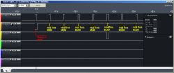
Thanks krzysiobal, I read your thread and now I am able to get the status bit to clear by toggling M2. With my setup, I was able to determine that the MMC5 is very likely to be counting falling edges of M2 for this purpose. I attached a photo explaining how I came to this conclusion, also described below.
I ran the exact same test, once with M2 being high when "in frame" gets asserted, and another time with M2 being low when "in frame" gets asserted, all the while with the CPU address bus pointing to $5204, R/W = 1, /ROMSEL = 1. I then inverted M2 repeatedly until I was able to read "in frame" status bit cleared.
With M2 initially high, I observed that the status must clear either after 2 falling edges or 2 rising edges of M2 (can't tell because you can't read the status with M2 low). With M2 initially low, I observed that it must clear in either 2 falling edges or 3 rising edges. Therefore, common denominator, it must clear in 2 falling edges.
Tomorrow, I will try to recreate the other observations you made, including reading from CPU addresses $FFFA/B and also the other 2 interrupt vectors.
If you have desoldered the MMC5, could you please check if pins 99 & 80 (GND) are internally connected, and same for pins 44 & 4 (VCC)
Also the behaviour of pin 56 (to RAM's VCC) should be examined - why RAM'S VCC is not connected straight to battery. Maybe there is some kind of brown-out detection, when battery's voltage (MMC5 pin 57) drops below certain level, MMC5 drives pin 56 to ground?
krzysiobal wrote:
why RAM'S VCC is not connected straight to battery.
Because all the switchover circuitry is inside the MMC5? They integrated a MM1026 or something similar inside the package.
I used a diode tester on the pins you mentioned. I am using this format:
Pin A -> Pin B
Where A is anode(+) and B is cathode(-) of the test.
VCC pins:
- 44 -> 4: 1.00V
- 4 -> 44: 0.99V
- 4 -> 56: 1.57V
- 56 -> 4: open
- 4 -> 57: 1.98V
- 57 -> 4: open
- 56 -> 57: 2.31V
- 57 -> 56: 1.41V
- 44 -> 57: 2.23V
- 57 -> 44: open
- 44 -> 56: 0.98V
- 56 -> 44: open
GND pins 80 and 99:
Measures 52 ohms or 0.04V diode test, same in both directions.
quickly throwing that in a table:
Code:
vcc4 v44 prgv batt <- to
vcc4 ---- 0.99 1.57 1.98
v44 1.00 ---- 0.98 2.23
prgv hi hi ---- 2.31
batt hi hi 1.41 ----
^from
Have to admit I'm surprised by many of these.
I quickly broke out my NES-ELROM-01 (4-44 shorted by PCB) board and measured a few things:
4+44 → 56 : 0.854V / 1.258V
4+44 → 57 : high / high
56 → 4+44 : high / 1.777V
56 → 57 : high / high
57 → 4+44 : 0.437V / 0.470V
57 → 56 : 0.559V / 0.618V
Two different voltmeters: the left one can't measure diode drops above 1V; the right can't measure diode drops above 2V.
Maybe pins 44/80 are digital vcc/gnd and 4/99 are analog vcc/gnd (used by the amplifier), cause they're all placed together.
krzysiobal wrote:
Maybe pins 44/80 are digital vcc/gnd and 4/99 are analog vcc/gnd (used by the amplifier), cause they're all placed together.
Exactly my theory as well.
I am doing some testing today on setting and clearing the "in frame" status bit. I have not yet tested reading from the vectors on the CPU bus. I have found results that confirm PPU /A13 involvement in setting this status bit. If /A13 = 1 (tested address 0x1FFF), it can set the status, and if /A13 = 0 (tested address 0x3FFF), it can't, except for the initial run with my setup. The status bit
does get set with PPU /RD falling edge when /A13 = 0 for the first run for me, so I am exploring that for an explanation. It would be easy to say "who cares" because it is just the first frame, but it could possibly shed some more clues.
I had suspected that PPU /A13 was latched somehow, as if the MMC5 is using the latched value for PPU /RD falling edge handling. The way my test was written, /A13 would actually start high and I would set M2 low before setting /A13 low. To test if M2 triggered /A13 to latch, I tried setting M2 low
after setting /A13 low. The status bit still got set first time, test fail.
Next, I tried toggling M2 before /RD falling edge. M2 initially high, then low - high - low. Status still got set. M2 high-low-high-low-high-low-high-low. STILL got set. Probably not M2's fault.
Next, I tried putting a 1k pull-down on /A13 so that it was never high from power on, and throughout the test, verified with oscilloscope that it stayed low. The status bit also still got set. This excludes the possibility that /A13 itself triggers its latch. Conclusion thus far: Whatever can latch /A13 apparently has not occurred yet before the first run of the test, and the default latch value is 1.
Next I tried adding a read of $5204, including toggles to M2, before doing the initial PPU /RD falling edge with /A13 low. Status bit still got set. So, the act of reading $5204 is not the trigger for this theoretical latch, and that kind of blows the whole latch theory because I don't do anything else for this test.
As best as I can tell so far, the initial falling edge of PPU/RD ignores /A13. Period.
I am not able to reproduce what I was saying with /A13 now -- I think I goofed something up. What I am seeing now is that the status bit initially gets set when PPU /RD goes low the first time, regardless of /A13. Then once cleared with M2 toggles, I can not get the status bit to set again after that no matter what the value of /A13. Sorry for the confusion on this -- my assumption was that I could set it again, depending on /A13, and wondering why the initial behavior was different. That seems to not be true now.
I need to go back and read your findings better krzysiobal. It looks like you figured all of this out already.
Quote:
I need to go back and read your findings better krzysiobal. It looks like you figured all of this out already.
There must be three PPU read cycles, all of them from the same address and and the address must be any from range $2000-$3fff.
I looked at how reading from CPU address $FFFA and $FFFB can clear the status. I verified it clearing with my setup. I found that the clearing of the bit is asynchronous. At any time that all of the following are true, it immediately clears the status bit:
- M2 = 1 (does not wait for an edge)
- /ROMSEL = 0
- CPU A14 through A3 = 1
- CPU A2 = 0
- CPU A1 = 1
- (CPU A0 = don't care.)
In addition, when I trigger the status bit to set with falling edge of PPU /RD, if I just leave PPU /RD low after that, I am still able to clear the status by reading $FFFA/B with PPU /RD remaining low the whole time.
It does not clear status when reading the other vectors from $FFFC - FFFF.
I don't know what the problem is, but I am not ever able to get the status bit to set again once I have cleared it. I hold the same PPU address and toggle PPU /RD a bunch of times, and the bit never gets set again. I tried with /A13 both high and low. I tried after clearing with $FFFA/B, and tried after clearing with M2 toggles. I only can get it to set 1 time after power up, which coincides with the
first falling edge of PPU /RD, regardless of PPU /A13. I verified with my scope that /A13 is being driven as intended. I am very confused!! Any ideas what I need to do to get the status bit to set a second time?
Well, right after I posted that I had a breakthrough on this.
I was using PPU addresses $1FFF and $3FFF. Both of those are not able to set the status bit. I tried $0000 and $2000, and $2000 IS able to set the bit again. I will continue this to figure out the exact address ranges that are able to set the bit.
I don't know why but just after power up, there need to be the following sequence:
ppu_read from address xxxx
ppu_read from address xxxx
ppu_read from address xxxx
cpu read 5204 <- it will return the in frame bit clear
ppu_read from any address
cpu read 5204 <- it will now set the in frame bit
After that, it status bit gets cleared, 3 ppu reads and then cpu read from $5204 will normally return in frame bit set (and now I checked that xxxx can be any from range $0000-$3fff, probably last time I misschecked something)
I started a long overnight test on each PPU address, should take many hours. When getting that test running, I found that as I changed things here and there, it took different numbers of PPU /RD toggles to set the status bit and different numbers of M2 toggles to clear the status bit. It didn't seem random - things were very repeatable. For the purpose of this test (i.e. identify all addresses that do and do not cause the status to set), I toggled each of those a bunch of times. There is definitely some counter business going on here. Will be interesting to poke more at it and to see if anything in this test indicates a connection between particular addresses and numbers of toggles.
Results from the test:
"In Frame" status bit is able to be set in the PPU address range $2000 - $3000.
Additional observations:
- As expected, PPU address $0000 did trigger the status bit to be set, based on prior knowledge that the first falling edge of PPU /RD always sets status regardless of PPU address.
- PPU address $3000 IS included. $3001 is the first one not to set the status bit in this test.
- Theory: It could be that after clearing in test $2FFF, the MMC5 has returned to it's "don't care about PPU address, just look for any PPU /RD falling edge" state. (Will test that.)
- PPU Address $2000 set the status on the 4th falling edge of PPU /RD
- All other addresses ($2001 - $3000 (including $3000)) set the status on the first falling edge of PPU /RD
- In this test, clearing of status always occurred on the 3rd falling edge of M2.
Yeah, there is some more complexity behind that, because not always three PPU read cycles set the bit (sometimes, one is just enough and sometimes four).
Now I can confirm that only $2000-$3fff adresses (when comes to three-cycle-read) are able to set the bit.
You were able to get the status bit to set with PPU address range $3001 - $3FFF? I tested each and every PPU address and gave 10 falling edges on PPU /RD, and nothing in that address range set the status bit for me.
My chip is marked MMC5A, is that what yours is marked?
Did a quick test, running PPU address range limited to just $2FF0 through $3003. Was able to repeat the status being set from beginning up to $3000 and then not set on $3001/2/3. I then made the test skip address $3000, so it tested $2FFE, $2FFF, [skipped], $3001. And the status did get set on $3001 this way and not on $3002. So it looks like it always is accepting the next one regardless of PPU address in this situation.
I am trying to keep in mind that this strange counter-type handling might be related to the difference between one scanline to the next vs. starting a whole new frame after v-blank. I might need to learn more about the PPU and how it accesses memory for different purposes.
That does smell like there's something off with your test. Try testing addresses randomly?
I have MMC5A from Just Breed.
Actually, the scanline counter is quite simple - at start of each PPU read cycle it just looks for the last three 3 PPU read addresses and whenever it sees three from same address, it increments its value.
What is also interesting is that even if the $5204.7 is set, /IRQ is asserted only if M2 toggles (if M2 stops toggling, it it deasserted) - same goes for the /IRQ asserted from $5209.
I just ran the same test except with random PPU address instead of sequential PPU address. I tested 10,000 random PPU addresses. The address range does correlate - the status bit could only get set in address range $2000 through $2FFF for me.
I noticed that in all cases after clearing the status, the next falling edge of PPU /RD always set the status again regardless of address, on the first falling edge. Will review the data more closely this evening.
Here is my data. I put some conditional formatting colors to make it easier to see. Some clear patterns emerge in this test.
I have found that the M2 counter for clearing status, resets its count any time PPU /RD has a falling edge, regardless of PPU address staying the same or changing. I found this by inserting PPU /RD toggles between each M2 toggle. It could never clear the status in this test.
Yes, that's how it works - there must be three or more CPU cycles without PPU read between to clear the in-frame bit.
Okay, my findings agree with that. You said 3 or more cycles -- not sure how literally you mean that. Have you seen it take more than 3 M2 falling edges to clear the status? I have only ever seen it take exactly 3 that I am aware of.
I still see a very persistent range of PPU addresses that can set the status which is different that yours:
$0000
-> Doesn't set
$1FFF
$2000
-> Does set after counting PPU /RD falling edges
$2FFF
$3000
-> Doesn't set for me, does set for you.
$3FFF
How can yours set in range $3000 - 3FFF but not mine? Do you write to any registers or drive any other inputs low at the beginning of your test?
Quote:
Okay, my findings agree with that. You said 3 or more cycles -- not sure how literally you mean that. Have you seen it take more than 3 M2 falling edges to clear the status? I have only ever seen it take exactly 3 that I am aware of.
I mean 3.
Quote:
How can yours set in range $3000 - 3FFF but not mine? Do you write to any registers or drive any other inputs low at the beginning of your test?
No, you are right, only $2000-$2fff can set it. I haven't checked that before with so many datails.
Okay. I am trying to think of this from the perspective of FPGA or CPLD, that is why I am so paranoid about edges and what latches and what happens asynchronously, etc.
Do you agree that the in-frame status bit works like this?:
Code:
// Declaration / initial values:
UInt16 prev_ppu_address = ? / don't care
bool always_set_in_frame_status_next_ppu_read = true; // Default true: first falling edge of PPU /RD always sets in_frame_status regardless of PPU address and set counter.
int set_counter = 0; // counts PPU /RD falling edges
int clear_counter = 0; // counts M2 falling edges
void on_ppu_rd_falling_edge( void )
{
clear_counter = 0; // Observation: Always resets M2 counter regardless if PPU address stayed the same or changed.
if(prev_ppu_addr != ppu_addr)
{
set_counter = 0;
prev_ppu_addr = ppu_addr;
}
if( true == always_set_in_frame_status_next_ppu_read )
{
in_frame_status = 1;
always_set_in_frame_status_next_ppu_read = false;
}
else if( ppu address is in range $2000 to 2FFF ) // Observed this range.
{
set_counter++;
if(set_counter >= 4)
{
in_frame_status = 1;
}
}
}
void on_m2_falling_edge (void)
{
if(in_frame_status = 1)
{
if(PPU /RD is high) // Observation: with PPU /RD held low, status can not clear with M2 toggles.
{
clear_counter++;
if(clear_counter >= 3) // Observation: always clears on the 3rd falling edge of M2, considering /RD had not reset the counter.
{
always_set_in_frame_status_next_ppu_read = true;
in_frame_status = 0
}
}
}
}
void combinational_logic (void)
{
'and' these:
M2, !(/ROMSEL), CPU A14,13,12,11,10,9,8,7,6,5,4,3,!2,1,in_frame_status
result 1 -> always_set_in_frame_status_next_ppu_read = true, in_frame_status = 0
// Observation: this part does not care about PPU /RD even if it is held low.
}
I am wondering if there is some way to simplify this - maybe the counters can be combined into 1 counter and the status bit is one of the bits of the counter, etc. I will think about it some more.
Edit:
Oops, nothing ever clears always_set_in_frame_status_next_ppu_read. hmmm...
Edit 2: fixed I think
I made a state diagram of how we think it works. I think this is a better approach than pseudo-code. I would like to try to verify each arrow in the diagram. If everything checks out, then I think we can feel pretty confident that we nailed down M2 and /RD interaction with the in frame status bit. Reading from CPU address $FFFA/B is not shown in this diagram.
Attachment:
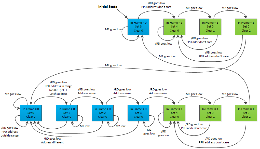 in_frame_bit_states.PNG [ 66.14 KiB | Viewed 4462 times ]
Edit: Something isn't right here because I know that you can loop through just the top 4 boxes if you keep reading PPU addresses in range 2000-2fff. This diagram shows the 4x /RD every other read even when PPU addresses remain in this range. Will think about how to fix the diagram.
Edit 2: This is better:
Attachment:
 in_frame_bit_states_2.PNG [ 80.42 KiB | Viewed 4449 times ]
Edit 3: This still isn't right because it alternates between caring and not caring about the PPU address when the address is always in range... I will get this, probably a few more revisions...
Edit 4: More improvements:
Attachment:
 in_frame_bit_states_3.PNG [ 82.18 KiB | Viewed 4443 times ]
Edit 5: I have looked at the diagram in edit 4 a fair bit now and I am feeling pretty good about it now. I think I will print it and start testing each arrow and checking them off.
New discovery:
It turns out that "RD Step 3" does not require a matching PPU address, or even a PPU address in range. In fact I set PPU address to 0x0000 and it still did the big loop around to the top. This finding removes 1 of the arrows from the diagram.
Attachment:
 in_frame_bit_states_4.PNG [ 80.85 KiB | Viewed 5619 times ]
Edit:
I have checked all arrows now and I believe that this diagram is correct. Additional things not shown or tested in this diagram:
- Any potential interaction with PPU /WR (none known)
- Reading from each of the 2 V-blank interrupt vector bytes from each of the 6 green boxes
- Any interaction with SL3 (pin 98), I am completely clueless on this one.
Edit 2:
I added the v-blank FFFA/B reads to the diagram. To make the arrows lay out better, I moved RD step 0.
Testing FFFA/B in each state divulged an interesting new connection from the 3rd /RD delay state back to the initial state. Normally, from state "RD step 3", falling edge of /RD always leads a 'good' sequence of green boxes (regardless of PPU address range), after which, another good or bad sequence of green boxes must also occur. However, if you sneak in a read from FFFA/B in "RD step 3", then it then it DOES matter if the PPU address is in range. It can go directly to the bad sequence of green boxes. This observation corresponds to a state change to the initial state.
The diagram did get a little more busy with the FFFA/B stuff added, but no previous findings were changed.
Attachment:
 in_frame_bit_states_5.PNG [ 100.88 KiB | Viewed 5611 times ]
Edit 3:
There is still more going on here with reading $FFFA/B. Say that I am in a "step 0" green box. The PPU address is in range and I don't touch it. Then I read CPU bus FFFA. I switch the CPU bus back to reading the status register and the status bit went to 0, as expected. Then on the 3rd falling edge of PPU /RD, the status gets set again. Coincidentally, this is the same spot it would have been set again going through the normal process of /RD delay had none of this ever happened, which leads me to believe the /RD delay states operate independently of what is going on elsewhere in this diagram. I tested this by reading FFFA within a "step 1" box. Now it was the 2nd falling edge to set the status again, which again coincides where it would have been set with normal /RD delay. I think this proves that the state of the RD delay must be operating independently from the other stuff that is going on.
I am thinking that this is going to blow up a little more complicated until we start to notice more patterns, then we can simplify it back down into its more general state of existence. I really truly believe that this is just a counter or two and some gates.
It is still pretty early on this new theory but it is making a lot of sense. I finally got rid of the duplicated 3 green / 1 blue box rows.
Attachment:
 in_frame_bit_states_6.PNG [ 76.83 KiB | Viewed 5594 times ]
Edit 1:
Issue found: The big top arrow on the gray boxes causes the /RD delay to always occur after any time the status bit is cleared. We have clearly observed the delay is skipped if the next PPU address is in range. So something is wrong with that arrow.
Edit 2:
Additional tweaks made:
Attachment:
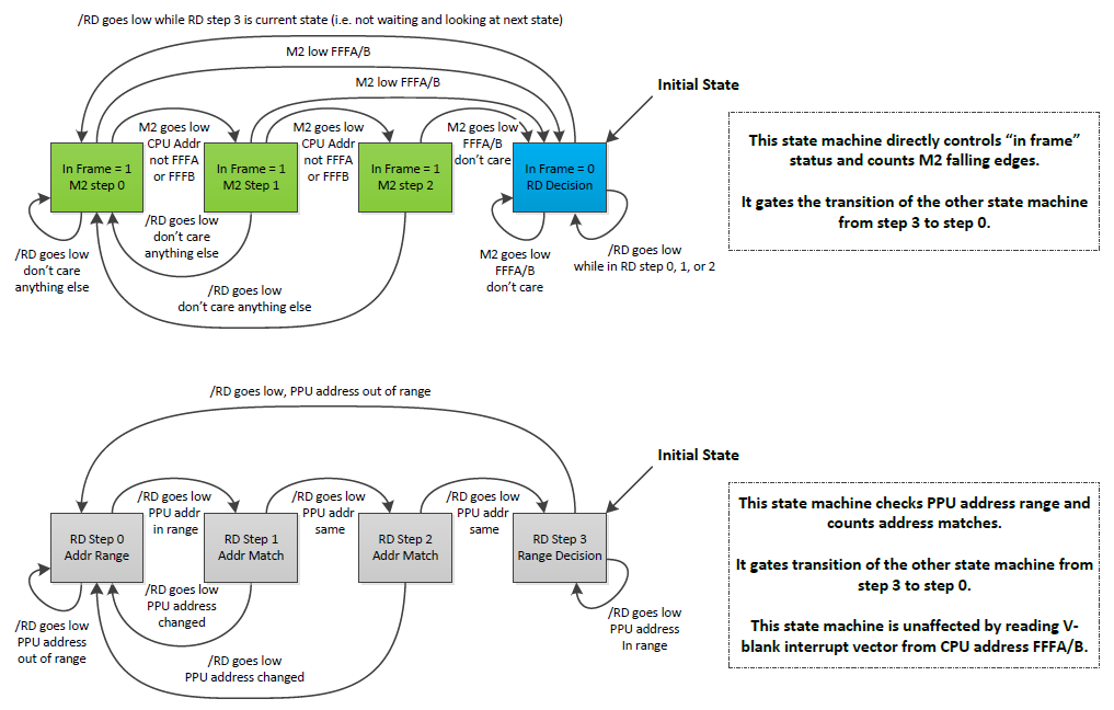 in_frame_bit_states_7.PNG [ 78.37 KiB | Viewed 5584 times ]
Edit 3:
I am still feeling pretty good about this one, except 1 observation I had before that is not captured. With PPU /RD held low, I observed that the status bit could not be cleared with M2 toggles. But with PPU /RD held low, it could be cleared with reading 0xFFFA/B.
Edit 4:
More tweaks per edit 3:
Attachment:
 in_frame_bit_states_8.PNG [ 73.19 KiB | Viewed 5572 times ]
Thanks for updating the arrows in my new MMC5 ASCII pinout in the wiki Lidnariq, I didn't realize how incomplete I left that!
Here are some tests that I did today to test the state diagram, especially focusing on reading from vblank interrupt vector address $FFFA. I am thinking that the diagram is just about exactly right now -- I am not able to find any example that disagrees with the diagram anymore. I have not tried anything with PPU /WR; maybe I should try toggling that pin from each state. I am open to any ideas for additional tests.
I am thinking it is quite likely that the clock of the top state machine is /RD 'and' M2. This would explain why /RD held low prevents M2 toggles from clearing status. If this is true, M2 step 1 should also not transition back to step 0 if M2 remains low after entering step 1, then /RD goes low and back high, and then finally M2 goes high. If true, 2 additional M2 falling edges with /RD high should clear the status in this case. I will test that tonight.
Test 1: RD state machine unaffected by reading FFFA/B, while in M2 step 0.
1. Set M2 = 1, R/W = 1, /RD = 1.
2. Get into this state:
*000
000*
- Set PPU address = $2000
- Set PPU /RD low and then high, 5 times
3. Set CPU address = $FFFA, then back to status register.
- Observation - status bit cleared.
Hypothetically, we are in this state:
000*
000*
4. Set /RD low (PPU address still $2000 and /RD still high since step 2.)
- Observation - status bit did set again right away.
*000
000*
Test 2: RD state machine unaffected by reading FFFA/B, while in M2 step 1.
1. Set M2 = 1, R/W = 1, /RD = 1.
2. Get into this state:
0*00
000*
- Set PPU address = $2000
- Set PPU /RD low and then high, 5 times
- Set M2 low and then high, once.
3. Set CPU address = $FFFA, then back to status register.
- Observation - status bit cleared.
Hypothetically, we are in this state:
000*
000*
4. Set /RD low (PPU address still $2000 and /RD still high since step 2.)
- Observation - status bit did set again right away.
*000
000*
Test 3: RD state machine unaffected by reading FFFA/B, while in M2 step 2.
1. Set M2 = 1, R/W = 1, /RD = 1.
2. Get into this state:
00*0
000*
- Set PPU address = $2000
- Set PPU /RD low and then high, 5 times
- Set M2 low and then high, twice.
3. Set CPU address = $FFFA, then back to status register.
- Observation - status bit cleared.
Hypothetically, we are in this state:
000*
000*
4. Set /RD low (PPU address still $2000 and /RD still high since step 2.)
- Observation - status bit did set again right away.
*000
000*
Test 4: RD state machine unaffected by reading FFFA/B, while in M2 step 3.
1. Set M2 = 1, R/W = 1, /RD = 1.
2. Get into this state:
000*
000*
- Set PPU address = $2000
- Set PPU /RD low and then high, 5 times
- Set M2 low and then high, 3 times.
- Observation - status bit on 3rd M2 falling edge.
3. Set CPU address = $FFFA, then back to status register.
- Observation - status bit stayed clear.
Hypothetically, we have remained in this state:
000*
000*
4. Set /RD low and then high (PPU address still $2000 and /RD still high since step 2.)
- Observation - status bit did set again right away.
*000
000*
Test 5: RD falling edge affecting step 3 in both state machines at the same time.
1. Set M2 = 1, R/W = 1, /RD = 1.
2. Get into this state:
*000
000*
- Set PPU address = $2000
- Set PPU /RD low and then high, 5 times
3. Set CPU address = $FFFA, then back to status register.
- Observation - status bit cleared.
Hypothetically, we have are in this state:
000*
000*
4. Set PPU address = $1FFF (different and out of range)
5. Set /RD low and then high (/RD had still been high since step 2.)
- In theory, the M2 state machine uses the "current state" of the RD state machine.
- Observation - status bit did set again.
Theory not disproved. Hypothetically, the current state is now:
*000
*000
6. Return to this state:
000*
*000
- Set CPU address = $FFFA, then back to status register.
- Observation - status bit cleared.
7. Set /RD low and then high (/RD had still been high since step 5, PPU address still $1FFF since step 4.)
- status remains cleared.
000*
*000
8. Set PPU address in range ($2000)
9. Set /RD low and then high 5 times
000*
0*00
000*
00*0
000*
000*
*000
000*
- Observation - Status became set on the 4th falling edge of /RD.
Okay, I am pretty sure I found something that does not match the "top state machine clocked by M2 'and' /RD" theory.

Test 1:
The test wrote:
PPU address = $2000 for entire test.
1. Get into this state, /RD and M2 high:
*000
000*
2. Set M2 low and keep it low. State should now be:
0*00
000*
3. Toggle /RD lots of times, ending up high. If the clock of the top state machine is /RD 'or' M2, states should be unaffected:
0*00
000*
4. Set M2 back high. States still unaffected
0*00
000*
5. Set M2 low and back high.
00*0
000*
6. Set M2 low and back high a 2nd time
000*
000*
Sure enough, this test passed, status went low after 2nd M2 toggle at the end.
HOWEVER: if I modify the test so that test step 2 starts in M2 step 2:
The test wrote:
PPU address = $2000 for entire test.
1. Get into this state, /RD and M2 high:
*000
000*
1b. Set skip to next state in top state machine by setting M2 low and back high once.
0*00
000*
2. Set M2 low and keep it low. State should now be:
00*0 (?)
000*
3. Toggle /RD lots of times, ending up high. If the clock of the top state machine is /RD 'or' M2, states should be unaffected:
00*0 (?)
000*
4. Set M2 back high. States still unaffected
00*0 (?)
000*
5. Set M2 low and back high.
000* <- status NOT cleared here, so it is not in this state.
000*
6. Set M2 low and back high a 2nd time
000* <- status did clear this time
000*
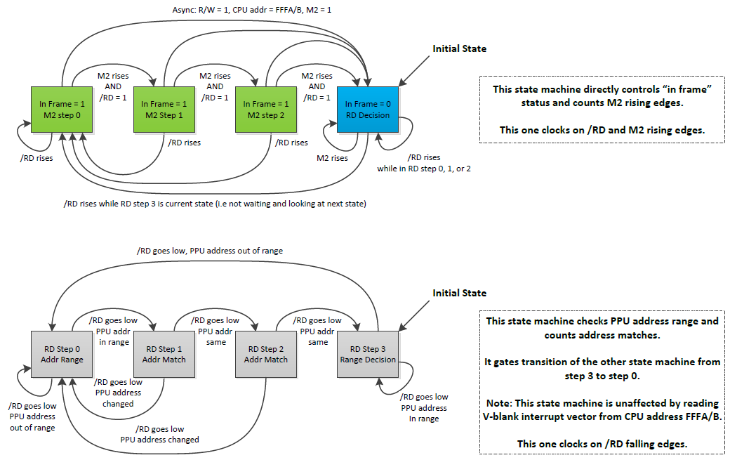
In this unrealistic situation, it takes 1 more M2 falling edge to clear the status bit than predicted. Though this condition can't probably happen in a real Famicom, it is still important because it shows us that our understanding is not yet complete.
Edit:
I don't feel good about it but here it is:
Attachment:
 in_frame_bit_states_9.PNG [ 77.34 KiB | Viewed 5512 times ]
It just doesn't feel right, the previous one felt better. I think I need to think about how to interpret those results and take a fresh look at the test tomorrow and make sure I didn't goof it up somehow.
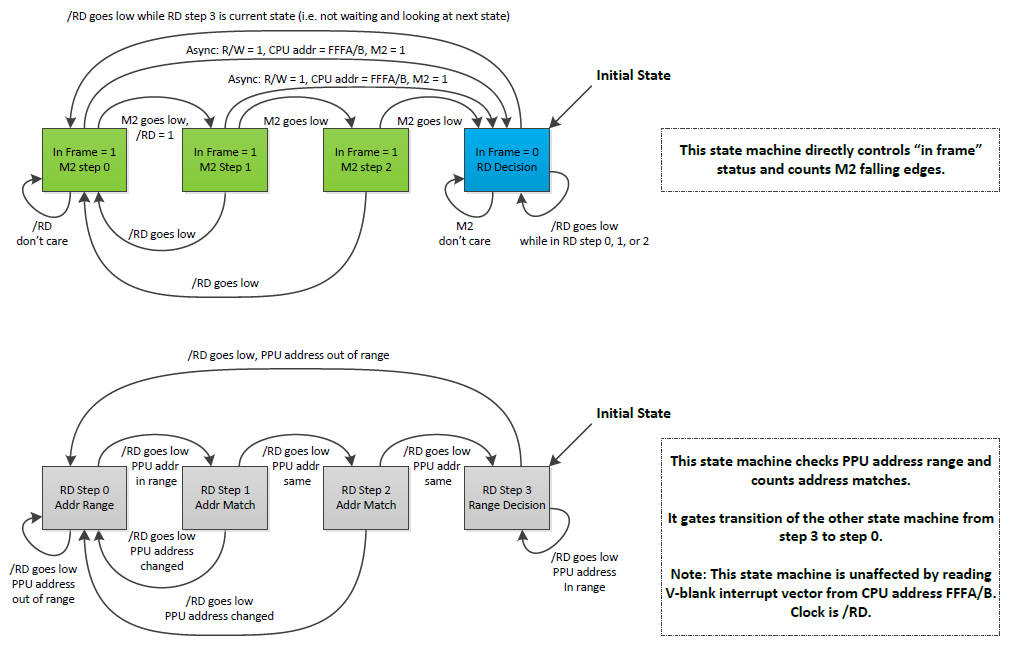
More testing is still necessary, but I have come up with a diagram that explains everything that I have observed so far, including 4 additional tests described below. This approach modified the top state machine to trigger on rising edge, and it left the bottom state machine triggering on falling edge. I did not yet test or think about the bottom state machine's edge in light of the changes to the top state machine. The triggering edge of M2 is tricky because you can't read the status with M2 low.
Attachment:
 in_frame_bit_states_A.PNG [ 77.17 KiB | Viewed 5475 times ]
It now passes all of these tests (below). Test 1, 2, 3, and 4 failed with previous diagrams.
All tests start in this state by setting PPU address = $2000 and toggling PPU /RD lots of times:
*000
000*
Test begins in this state with M2 = 1, /RD = 1, status bit set.
Control Test (already passed) wrote:
- M2 falls
- M2 rises
- M2 falls
- M2 rises
- M2 falls
- M2 rises <- status bit got cleared here.
Test 1 wrote:
- M2 falls
- RD fall and rise lots of times, ending high
- M2 rises
- M2 falls
- M2 rises
- M2 falls
- M2 rises <- status bit got cleared here.
Test 2 wrote:
- M2 falls
- M2 rises
- M2 falls
- RD fall and rise lots of times, ending high
- M2 rises
- M2 falls
- M2 rises
- M2 falls
- M2 rises <- status bit got cleared here.
Test 3 wrote:
- M2 falls
- RD falls
- M2 rises
- RD rises
- M2 falls
- M2 rises
- M2 falls
- M2 rises
- M2 falls
- M2 rises <- status bit got cleared here.
Test 4 wrote:
- M2 falls
- M2 rises
- M2 falls
- RD falls
- M2 rises
- RD rises
- M2 falls
- M2 rises
- M2 falls
- M2 rises
- M2 falls
- M2 rises <- status bit got cleared here.
New problem. It seems like I have just fixed some complicated status clearing sequences, but one of the first things I knew about this was that PPU /RD falling edge sets the status, and that seems to have broken in this latest diagram. I need to verify that is true, and if so, make more changes to the diagram. I have been toying with the idea that the top state machine only clears and the bottom state machine only sets. I think I will think about that idea some more.
I am really impressed in the way you analyze this, but I personally thing that this complexity might be some kind of implementations's side effect how status setting was meant to work.
if I were you, I wouldn't spend on it so much time, there are many other interesting aspects of MMC5 to analyze and replicationg exactly that status bit behaviour will be hard too.
Thanks krzysiobal. I feel like I am still getting closer on this status bit -- as it is, I think this diagram is very good at explaining the behavior, but there are still some corner conditions that don't quite match up yet. I think that there is more I can do with this bit before feeling good about it and moving on to something else. These issues could potentially make graphical glitches if implemented this way. I want my trippy backgrounds to be perfect.

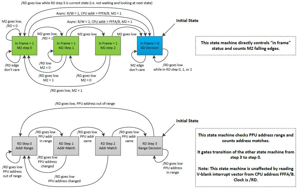
I mentioned my idea where the top state machine clears status and the bottom one sets status, but the interaction of PPU /RD falling edge causing a state change in both state machines at the same time is really integrated into my observations so far. That feature really explains a lot of what we see here, so it is hard to consider giving that up. A new idea I had over lunch today was that maybe all of the PPU /RD logic in the top state machine operates asynchronously, similar to reading $FFFA/B. I think I can test that theory like this:
- Get into this state, just like recent tests:
*000
000*
status = 1, /RD = 1, M2 = 1 - Never touch M2 in this test.
- Set PPU /RD low, leave it low.
- Read $FFFA. It should put us into this state:
000*
000* - Read status. If /RD logic is asynchronous like $FFFA, status should automatically set and we should be in this state:
*000
000* - If status is still not set, rise /RD, check status again. If it got set, it waited for rising edge PPU /RD.
- If status is still not set, fall /RD, check status again. If it got set (It definitely should be set by now), it waited for falling edge PPU /RD.
Will try it later tonight.
Edit:
It definitely waited until the last step to set the status bit. It apparently does wait for a PPU /RD falling edge, not asynchronous.
In other news, I recently hooked up an LED bargraph display to all 8 unknown pins. I keep an eye on it for any blinks/flashes during these tests now. All 8 have always been output high or open bus (can't tell the difference with this setup) so far.
Edit 2:
I looked into the /RD edge trigger of the top state machine. We know for a fact that exiting the blue box and going back to M2 step 0 happens on the falling edge of /RD. However, due to the 'and' logic with /RD when stepping from M2 step 0, 1, 2, it might not be possible to tell for certain which edge of /RD takes you from M2 step 1 to step 0, or M2 step 2 to step 0. It actually might not
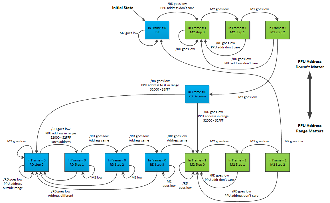
matter. We do know that /RD is falling edge when exiting the blue box, so in keeping with this, I made all /RD falling edge and all M2 rising edge. I feel pretty satisfied with this diagram now -- I think that it accurately describes the status bit. I think we are good enough with this bit now to proceed to other MMC5 things, definitely in agreement with you krzysiobal. Here is the final 'in frame' status bit diagram, for now anyway.
Attachment:
 in_frame_bit_states_B.PNG [ 75.45 KiB | Viewed 5407 times ]
I think I could put this diagram in the wiki. What should I look at next?
On the topic of the IRQ-related register at $5209, is there any possibility that it's actually a cycle counter initialized by writing to $5207-$5208? Having a register that just triggers an IRQ when you write to it seems slightly useless, at least in my opinion.
I agree, that does seem sort of useless without some cycle counting or something, very similar to the DAC interrupt. Why would you need an interrupt if you already know it is going to happen immediately? It seems like there may be more to these things. I will try poking at it some time soon.
I am interested to see this done.
Quietust wrote:
On the topic of the IRQ-related register at $5209, is there any possibility that it's actually a cycle counter initialized by writing to $5207-$5208? Having a register that just triggers an IRQ when you write to it seems slightly useless, at least in my opinion.
Lol, you are correct. Writing value X to $5209 causes interrupt to trigger on X-th rising edge of M2. Because M2 needs to be toggled constantly, I did not realise that before. And writing value 0 never triggers interrupt, probably because it is triggered when counter clockes from 1 to 0.
Though, only 8 bit M2 counter seems to be hardly useful. I wonder where to write high byte
Also, when M2 stops toggling, around 11us from that time MMC5 is bring to reset (causing interrupt line to go high)
Coooool! That is a super nice feature that nobody knew about! You could use that timer interrupt to write raw DAC samples!! That discovery is GOLDEN

My setup can't toggle M2 that fast so I would not have been able to test this. Did you try writing anything to $520A? In keeping with the multiplier result being in little endian, it seems that the high byte (if existing) might come after the low byte for this too.
Edit:
Additional questions about this register while the timer is running, before the IRQ happens (ex. writing a big value like $FF so you have time to try stuff):
- What happens if you read register $5209? Is there a different flag to show that it is running?
- How about reading register $5208 while it is running? Is it still reporting $C0?
- What happens if you write value $01 - will it reload the counter and have the IRQ next rising edge of M2, or continue counting from the original value you wrote?
- What happens if you write value $00 - does it cancel the timer and never generate the IRQ?
If it matters, I seem to remember there being multiplication algorithms that generate 2 bits per iteration. Multiplying two 8-bit numbers would converge in 4 iterations, which at 1 cycle per iteration is the time from a write to the following read.
I think that does matter tepples -- that method could save a lot of resources when trying to replicate MMC5 in hardware.
I was not able to ever observe an incomplete product, but I was testing extremely slow and I was toggling M2 during the test, which I am not sure is necessary or not. I didn't try it without toggling M2. Since, to your point, the NES could not possibly expect to read the result until some cycles later, it definitely seems reasonable to implement a multiply that relies on that fact -- whether or not a real MMC5 technically does it faster.
Quote:
What happens if you read register $5209? Is there a different flag to show that it is running?
It read backs as $00. After the X-th edge it read backs as $80 (and reading it clears pending interrupt).
Interrupt is reported around 41ns after rising edge of M2 and it is cleared also around 41ns after falling edge of M2 of the "read $5209" cycle.
If the X-th cycle is "read $5209" then the interrupt is reported only for the period of time between rising and falling edge (as below).
And it counts M2 cycles (no matter if this is read or write cycle)
Quote:
How about reading register $5208 while it is running? Is it still reporting $C0?
Yes, before/on/after X-th edge it is still $C0
Quote:
What happens if you write value $01 - will it reload the counter and have the IRQ next rising edge of M2, or continue counting from the original value you wrote?
IRQ will be triggered on the next rising edge of M2
Quote:
What happens if you write value $00 - does it cancel the timer and never generate the IRQ?
Yes. But if the IRQ is already pending, writing $00 to $5209 does not cause it to acknowledge.
And yes, $520A is used to write upper 8 bits of the counter.
And no, $520B is not upper 16-23 bits (counter is only 16 bits wide)
krzysiobal wrote:
And yes, $520A is used to write upper 8 bits of the counter.
Do writes to $5209 start the counter, then? Or does it just count while nonzero, and certain values are harder to request?
krzysiobal wrote:
And yes, $520A is used to write upper 8 bits of the counter.
And no, $520B is not upper 16-23 bits (counter is only 16 bits wide)
Great work!!


krzysiobal wrote:
And yes, $520A is used to write upper 8 bits of the counter.
And no, $520B is not upper 16-23 bits (counter is only 16 bits wide)
Presumably, writing $01 to $520A and then $00 to $5209 will generate an IRQ after exactly 256 cycles.
Next things to figure out:
1. Does it matter in what order you write the values to $5209-$520A? (i.e. will the sequence $01 -> $520A, $80 -> $5209, $02 -> $520A trigger an IRQ after 384 cycles or after 640 cycles?)
2. What exactly, then, is at $5207-$5208?
lidnariq wrote:
krzysiobal wrote:
And yes, $520A is used to write upper 8 bits of the counter.
Do writes to $5209 start the counter, then? Or does it just count while nonzero, and certain values are harder to request?
It seems that only writing to $5209 starts the counter. That is, the following sequence:
write($5209, 0)
write($520A, 0)
write($520A, 1)
will not start counter, but the one below will:
write($5209, 0)
write($520A, 0)
write($520A, 1)
write($5209, 0)
Also, when the counter is ticking, writing to $520A will cause its value to be modified so there are no temporary registers:
write($5209, $5)
write($520A, $1)
write($520A, $ff) <- it will immediatelly update counter high byte
I did a not-so-exciting test on $5207 / $5208 last night. I wrote all possible combinations of data to registers $5207 and $5208 and I didn't read anything other than $C0 from $5208 from the entire test.
It went like this:
Code:
Init:
R/W = 1 (read from MMC5)
M2 = 1 (allow reading and loading new data)
for( int i = 0x0000, i <= 0xFFFF, i++ )
{
// Write low byte of i to $5207
Record low byte of i to spreadsheet
CPU address = $5207
R/W = 0 (write to MMC5)
Set logic analyzer to output to CPU data bus
Set data bus to low byte of i
M2 = 0 (register the data)
M2 = 1 (allow reading and loading new data)
// Read back register $5208
Set logic analyzer to input from CPU data bus
R/W = 1 (read from MMC5)
Record data bus value to spreadsheet
// Write high byte of i to $5208
Record high byte of i to spreadsheet
CPU address already = $5208, no action
R/W = 0 (write to MMC5)
Set logic analyzer to output to CPU data bus
Set data bus to high byte of i
M2 = 0 (register the data)
M2 = 1 (allow reading and loading new data)
// Read back register $5208
Set logic analyzer to input from CPU data bus
R/W = 1 (read from MMC5)
Record data bus value to spreadsheet
}
Edit:
Running the same test again but now reading register $5206 each time. If any combination of values written to $5207 / 5208 should turn the multiply into a signed multiply, $5206 should become $00 instead of $FE.
$FF(unsigned: 255) * $FF(unsigned: 255) = $
FE01(unsigned: 65025)
$FF(signed: -1) * $FF(signed: -1) = $
0001(signed: 1)
Seems doubtful but worth a try.
Edit 2:
Result: $5206 was always $FE during every step of that test. We can probably say that no combination of inputs to the multiplier affect the readback value of $5208, and no combination of inputs written to registers $5207 or 5208 affect the result of the multiplier.
Out of curiosity, have you tried just generically fuzzing the MMC5? Write random values randomly all over the $5000-$52FF range and see if $5208 changes?
I don't know why but I have a premonition that $5208's value might be in connection to some hardware aspect of chip:
* How MMC5 is wired (SL/CL mode)
* Voltage of the battery (pin 57)
* Revision
lidnariq wrote:
Out of curiosity, have you tried just generically fuzzing the MMC5? Write random values randomly all over the $5000-$52FF range and see if $5208 changes?
Great idea, I will try it.
krzysiobal wrote:
I don't know why but I have a premonition that $5208's value might be in connection to some hardware aspect of chip:
* How MMC5 is wired (SL/CL mode)
* Voltage of the battery (pin 57)
* Revision
Cool theories. For the idea of revision, it seems that both of us have chips marked MMC5A. Do you have any other MMC5 carts that might have the non-A version? I will dig a bit but I am almost sure I do not have any others.
My setup has battery removed. Do you still have the battery installed in yours?
My setup has SL/CL disconnected. Are yours connected?
I have an MMC5letterless cart, but no testing apparatus.
Do you have a ROM dumper? $5208 should be easily dumpable.
In other news, it seems there is some sort of locking function. At the beginning of my test, bankswitching of CHR was occurring quite frequently with random writes to random addresses in the range $5000-$52FF, then all of a sudden it got stuck and has remained stuck for a long time now. I think I will let it go and see if it will unstick itself by morning - could be interesting. Maybe the MMC5A "crashed" somehow, that would have interesting implications to consider if it is crashable. Hopefully it doesn't have firmware in there that I just wiped out. That seems pretty doubtful for the mid 1990s I guess but you never know.
I plan to review the data between the last successful bankswitch and the next time that it should have done a bankswitch, and see what happened between there. As of yet, I have seen no changes to the unknown pins or to register $5208.
Edit:
I gave in and power cycled the MMC5 and restarted the test. It functions normally again, but it does seem to lock up quite quickly from this test. I might try playing with the random address range written to and see if I can narrow down any particular addresses that cause this locking. In both lock-ups, it ended up with CHR address pointing thusly: CHR A19 and A18 = 0. CHR A17 to A10, A2 to A0, CL3, SL3, all equal 1. PRG A19 to A13 all equal 1 (not sure they ever changed though to begin with though). Definitely no changes to the unknown pins in this test. They all remained either driven high or hi-z (can't currently tell the difference).
Edit 2:
Changing my random address range to be $5120 to $512B, it locked up almost immediately. Reducing the range to $5120 to $512A allowed the PPU bank to keep dancing all over indefinitely. So, writing to $512B can cause the lockup of the PPU bank. Maybe it is waiting for additional PPU reads, etc - I am not familiar with this.
Then, specifically excluding $512B from address range $5000 to $52FF, it still was able to lock up. I then excluded the range $512B to $512F, and now it does not lock up. Therefore, there is at least 1 more register in that range that behaves similar to $512B. The test is now set up to run all night, avoiding this address range. I should have a million or so random writes and dumps of all pins by morning.
Edit 3:
Lidnariq: I went ahead and ordered up 2 cheap Famicom L'Empereurs, hopefully one of them will have a non-'A' MMC5.
You should make all addres line / RnW changeswhen M2 is 0 and put M2 to 0 after end of cycle, otherwise you are risking doing extra read/write cycles. Unfortunatelly from the code example, you are doing the opposite.
Maybe when M2 stops cycling, also all of its banking settings does to default?
---
All the test were done without battery, but when I plug battry into the socket, nothing changed concerning $5208.
---
BINGO! I still does not know the role of pin 98 and 97 (if that switches between CL and SL mode, why there is just not one input pin that connects between VCC and GND?).
Nevermind, I cut the CL3 jumper (which connected MMC5.98 with MMC5.97). Now both of them are not connected to anything. Reads of $5208 still returns C0.
But both of the pins seems to be inputs (with pullups to VCC). When both of them are not connected to anything, there is 5V on them, but after shorting any of them to GND (with even weak serial 4.7k resistor, the voltage drops to ~0.2V, so they must be inputs)
Shorting any of them to GND alters the value returned by $5208:
Code:
[AB00 0000] $5208 (reading)
||
|+---------- value of MMC5.97 pin
+----------- value of MMC5.98 pin
Now there need to be figured out:
* Does changing vale of those pins alters any MMC5 behaviour or
* are just they some kind of DIP swithes that game can readback (like in MAPPER90 games)
Wiki says that:
Quote:
In other words, CL mode passes the lowest PPU address bits straight to CHR ROM, while SL mode runs them through MMC5. SL mode allows the MMC5 to perform smooth vertical scrolling in split mode, while CL mode does not. Nearly all MMC5 cartridges use CL mode - it is not known why SL mode was not used instead: possibly ROM speed issues.
But I analyzed all the MMC5 PCBs from botgod and no single one uses SL mode.
Oh cool - I am glad you were able to figure that out, and thanks for sacrificing your CL3 jumper.
I genuinely did not know that the right time to make address changes was when M2 is 0. I will do that from now on.
It looks like the CHR banking is not reset from stopping M2 toggling. Since my PPU address bus is just floating, which ends up all 1s, I am not getting a very good representation of the actual banking that is going on, but the extended CHR address bits do flip one way, stay for a while, flip the other way, stay for a while, during this test. If it was resetting, I think it would mostly stay the same, and show little glitches as it changed and reset back right away.
I never did witness the PRG banking change (haven't checked the results this morning yet), so it makes sense that one is reset by delay in M2. I would probably not have seen the said glitches on the extended PRG bits unless I had my scope hooked to them or something.
Edit:
krzysiobal wrote:
Wiki says that:
Quote:
In other words, CL mode passes the lowest PPU address bits straight to CHR ROM, while SL mode runs them through MMC5. SL mode allows the MMC5 to perform smooth vertical scrolling in split mode, while CL mode does not. Nearly all MMC5 cartridges use CL mode - it is not known why SL mode was not used instead: possibly ROM speed issues.
But I analyzed all the MMC5 PCBs from botgod and no single one uses SL mode.
The wiki also said that there are 2 versions of MMC5: "MMC5" and "MMC5B". I think we have some work to do on the wiki. As we find things that seem somewhat conclusive, I have been (and I will continue to) add them on there as we go.
I will play around with CHR address ranges and see if I can affect either of these pins. They could be bi-directional pins. It seems quite odd to connect together 2 inputs, and not connecting them to gnd or vcc. There must be something more to that.
Edit 2:
In summary of the test, the only pins that ever changed after over 1,000,000 writes were the bankswitched CHR address bits. None of the unknown pins, and none of the PRG address bits. I had all PPU address bits = 1 the whole time.
The CPU address bits were being controlled to do the writes and reads, and at the time of sampling these bits, the CPU address would always have been $5208.
Looking at the writes in the range $5120 to $512A that caused a CHR bankswitch:
Code:
Range $5120 - 5127:
A19 A10 SL3 CL3 A2 A0
| | | | | |
0011 1111 11 1 1 111
Range $5128 - 512A
A19 A10 SL3 CL3 A2 A0
| | | | | |
0000 0000 00 1 1 111
I got a reasonably even distribution of writes that triggered the change of A17 through A10, also really even distribution of the value that was written. I did observe one single write of $00 that triggered a bankswitch, but my test observed no write of value $FF that triggered it. It is completely possible that the random test just never hit that combination.
5120: 31
5121: 21
5122: 28
5123: 25
5124: 23
5125: 17
5126: 19
5127: 21
5128: 70
5129: 58
512A: 56
Ben Boldt wrote:
krzysiobal wrote:
But I analyzed all the MMC5 PCBs from botgod and no single one uses SL mode.
The wiki also said that there are 2 versions of MMC5: "MMC5" and "MMC5B".
Nah, we know that there are a very finite number of PCBs that used the MMC5 and all four of them per region left it in CL mode.
If there were dedicated prototyping boards made for the MMC5 (ETPROM?) maybe those support it. But we haven't found any yet.
The CL/SL mode stuff has been on the MMC5 pinout wiki page since its creation by user
Banshaku in 2009. Are you around for comment Banshaku?
I tried putting a 10k pull-down on each of the unknown pins, and I found the following voltage clues:
- VCC 5.01V
- Pin#, Open Voltage, 10k to Gnd voltage
- 94 (CHR A0), 5.01, 4.96 <- Clearly driven high
- 74 (PRG /CE), 5.01, 4.97 <- Clearly driven high
- 70 (PRG RAM A14), 5.01, 4.97 <- Clearly driven high
- 73 (unknown), 5.01, 4.97 <- Clearly driven high
- 93 (unknown), 5.01, 4.96 <- Clearly driven high
- 76 (PRG RAM /WE) 4.96, 3.17
- 72 (PRG RAM 1 /CE), 4.96, 3.17
- 71 (PRG RAM 0 /CE), 4.96, 3.17
- 75 (unknown), 4.96, 3.17
- 30 (unknown), 5.00, 1.94
- 29 (unknown), 5.00, 1.93
- 92 (unknown), 5.00, 1.86
- 82 (unknown), 5.00, 1.85
- 81 (unknown), 5.00, 1.72
- 28 (PPU A13), 4.96, 0.89 <- Input
- 98 (SL3), 4.99, 0.90V <- Input
- 97 (CL3), 4.99, 0.90V <- Input
Edit:
verified that DAC is indeed coming out from Pin 2. I characterized the voltage to DAC value here:
https://wiki.nesdev.com/w/index.php/MMC ... .245011.29
Ben Boldt wrote:
The CL/SL mode stuff has been on the MMC5 pinout wiki page since its creation
It was just copied from kevtris's documentation
here.
lidnariq wrote:
Ben Boldt wrote:
The CL/SL mode stuff has been on the MMC5 pinout wiki page since its creation
It was just copied from kevtris's documentation
here.
Okay. Where do you think he got that info from? How would he know that it has to do with split-screen scrolling? To me, looking at Just Breed's PCB, all of the jumpers that are closed are labeled CLx and all of them that are open are labeled SLx (where x is a number). It looks like for each x, there is a pair of CLx and SLx always near each other. If CL and SL are to be overall modes of the MMC5, it might shed some light to think about the overall differences when opening all of the CLx and closing all of the SLx -- not just CL3 and SL3.
Well, we know by inspection that CL4-6 and SL4-6 connect CHR A0-A2 to PPU A0-A2, or instead go via the MMC5.
And the only known behavior that could use that is the left-and-right split screen. (Or flipping background tiles vertically, but that's evidently not present)
Similarly, we know what SL2/CL2 (battery backup of RAM), SL1/CL1 (battery backup of second RAM), and SL15/CL15 (enables two 32KiB RAMs on NES-ETROM) do.
As to whether Kevtris assumed something, or was citing some even older source ... don't know. You might be able to get in touch with him via IRC.
lidnariq wrote:
And the only known behavior that could use that is the left-and-right split screen.
Okay, that explains a lot. I admittedly had not even looked at where any of the jumpers connect yet, but I would not have been able to see the relation to split screen anyway. Thanks for your experience on this. So basically, swapping several CLx/SLx pairs appears to be the idea kevtris was already going on, possibly with the same assumptions that I was suggesting.
I guess the pins named CL3 and SL3 are right next to CHR A0, A1, A2, and these 3 address bits point to the split screen business. That does seem a pretty strong indication that they are directly related. In case they aren't, it is easy for me not to get stuck on that relation because I don't understand it anyway!

I research it with a truly open mind.

Ben Boldt wrote:
I guess the pins named CL3 and SL3 are right next to CHR A0, A1, A2, and these 3 address bits point to the split screen business. That does seem a pretty strong indication that they are directly related. In case they aren't, it is easy for me not to get stuck on that relation because I don't understand it anyway!
Unfortunately, they're not. (Much to my disappointment/surprise)
4-6 are vaguely in the middle of the PCB, between CHR and the MMC5.
1 and 2 are next to their corresponding PRG RAM
15 isn't particularly near anything, between PRG ROM and PRG RAM
but 3 is off in the corner near the battery in HVC/NES-E{K/T/W}ROM.
HVC/NES-ELROM might be the exception that led to the impression. On these PCBs 3 is vaguely near 4-6.
I think I would like to set up a test that has random PPU addresses, writes and reads, and monitors CHR A0, A1, A2, CL3, SL3, and especially Unknown Pin 93.
I measured the voltages of all pins today with and without a 10k pull-down. Only PRG RAM /CE /WE -related pins do the 3.17V thing measured on pin 75. That is a good clue that 75 relates to those.
73 and 93 act like ordinary output high seen on lots of pins. Our best clues are proximity to other pins. 73 measures like 74 (PRG /CE), also 93 measures like 94/95/96 (CHR A0/A1/A2).
Pins 29, 30, 81, 82, and 92 all have this weird 1.8V business not seen on any known pins.

It works out to an 18k internal pull-up. It could mean that those pins are related to each other, or it might not be a good sign that those pins actually do anything... But at least 73/75/93 look promising.
I did some more DAC testing and came up with a more general equation that considers AVcc:
Pin 2 Voltage = [(DAC value / 255) * (0.4 * AVcc)] + (0.1 * AVcc)
Attachment:
 dac characteristic.png [ 38.98 KiB | Viewed 2690 times ]
I updated the
Wiki with this.
I keep dreaming about the DAC being able to play by itself out of the MMC5's internal RAM, and then interrupt when done. That would be so cool.
If you leave AVcc floating, but supply +5V on DVcc, what voltage appears on AVcc?
lidnariq wrote:
If you leave AVcc floating, but supply +5V on DVcc, what voltage appears on AVcc?
And try to measure the internal resistance of that output too.
lidnariq wrote:
If you leave AVcc floating, but supply +5V on DVcc, what voltage appears on AVcc?
Flat zero.
krzysiobal wrote:
And try to measure the internal resistance of that output too.
Will do. DACs typically are made out of big resistor networks so I will consider that and test different conditions, etc.
Edit:
It looks to have a current-limited output at about 173 uA:
Attachment:
 dac impedance.png [ 14.38 KiB | Viewed 2664 times ]
I calculate the maximum non-distorted load to be 14.45 kohm to gnd. I am not sure if it hurts it to enter current-limit mode, so I only applied the load momentarily for each point to read the meter, then took it away.
Edit 2:
I have more work to do on this -- The current limit depends on AVcc. The graph shown is with AVcc = 5V. I tried reducing AVcc to 3V and it current limited to 0.720 volts with the 8.03k resistor.
Edit 3:
Attachment:
 dac current limit vs. AVcc.png [ 13.21 KiB | Viewed 2663 times ]
Wait, so the MMC5 DAC is linear? That means it's not just a repackaged APU.
Do you have any plans to measure the pulse channels? I'm not hardware-savvy enough to tell if that's feasible with your setup.
Rahsennor wrote:
Wait, so the MMC5 DAC is linear? That means it's not just a repackaged APU.
We've known for a long time that the MMC5's pulse channels aren't just a repackaged APU, and the presence of a linear DAC would just be
one of the reasons. Another would be the lack of pitch sweeping support (which isn't surprising, because they took up about 1/3 of the RP2A03 pulse channels' die space), and yet another would be the fact that the RP2A03 and MMC5 use inherently different processes (the former is depletion-load NMOS, while the latter is CMOS).
Still, replacing the DAC would've been trivial even if the MMC5
did use a direct copy of the NES APU, since it's only a single isolated component of it - in
Visual 2A03, the Pulse DAC is just the region enclosed by t10283 and t10311, and the Triangle/Noise/PCM DAC is just the area within t13792 and t14502.
Quietust wrote:
MMC5 use inherently different processes [...] while the latter is CMOS
We know it's CMOS?
lidnariq wrote:
Quietust wrote:
MMC5 use inherently different processes [...] while the latter is CMOS
We know it's CMOS?
I suppose we technically don't know 100% for certain, so I retract that particular statement.
Do we have any insinuation that it's CMOS?
I assumed it was NMOS because inputs source current, so if there's any evidence any direction I'm curious to hear about it.
Rahsennor wrote:
Wait, so the MMC5 DAC is linear? That means it's not just a repackaged APU.
Do you have any plans to measure the pulse channels? I'm not hardware-savvy enough to tell if that's feasible with your setup.
I could try that. I am thinking that the M2 reset detection would probably stop the pulse channels, so as to prevent stuck notes when you reset the Nintendo, so that might be a problem with my setup. I might try using a function generator into M2 to get around this.
I am not quite set up for fast M2 yet, I have to think about it a little bit more and get that going before I can look at the pulse channels. In the meantime, I tried writing to the MMC5's built-in RAM. Something isn't working right. I always read back all 00s from the RAM. Could you guys review my test code and let me know anything you notice? Especially consider how I am handling M2 and R/W edges - I don't have a good handle on the correct sequence of those yet. Are there more modes I need to set or unlocks that I need to do? Or could my slow M2 be screwing this up somehow? Hopefully not.
Code:
private void testFillRam()
{
byte data_to_write = 0x10;
string s = "";
readAndRefreshGraphics();
// Set CPU R/W, /ROMSEL, and M2 as outputs:
sendDataDirection(0xF8, 0x4A, 0);
// Set these outputs to high:
setCpuRW(true);
setRomSel(true);
setM2(false);
// Send
sendOutput(logicData[5][0], 0x4A, 0);
// Set CPU address bus as output:
sendDataDirection(0x00, 0x42, 0);
sendDataDirection(0x00, 0x42, 1);
setCpuRW(false);
sendOutput(logicData[5][0], 0x4A, 0);
// Set CPU data bus as output:
sendDataDirection(0x00, 0x46, 0);
// Write value $02 to register $5102:
setCpuAddress(0x5102);
sendOutput(logicData[1][0], 0x42, 0); // LSB
sendOutput(logicData[1][1], 0x42, 1); // MSB
logicData[3][0] = 0x02; // Data to write
sendOutput(logicData[3][0], 0x46, 0);
setM2(true); // Register the data
sendOutput(logicData[5][0], 0x4A, 0);
setM2(false);
sendOutput(logicData[5][0], 0x4A, 0);
// End set $5102 to unlock value $02:
// Write value $01 to register $5103:
setCpuAddress(0x5103);
sendOutput(logicData[1][0], 0x42, 0); // LSB
sendOutput(logicData[1][1], 0x42, 1); // MSB
logicData[3][0] = 0x01; // Data to write
sendOutput(logicData[3][0], 0x46, 0);
setM2(true); // Register the data
sendOutput(logicData[5][0], 0x4A, 0);
setM2(false);
sendOutput(logicData[5][0], 0x4A, 0);
// End set $5103 to unlock value $01:
// Write mode value $02 to register $5104:
setCpuAddress(0x5104);
sendOutput(logicData[1][0], 0x42, 0); // LSB
sendOutput(logicData[1][1], 0x42, 1); // MSB
logicData[3][0] = 0x02; // Data to write
sendOutput(logicData[3][0], 0x46, 0);
setM2(true); // Register the data
sendOutput(logicData[5][0], 0x4A, 0);
setM2(false);
sendOutput(logicData[5][0], 0x4A, 0);
// End set $5104 to mode 02 (normal RAM)
// Start: write non-zero, non-FF, non-negative data to entire expansion RAM:
for (int i = 0x5C00; i < 0x6000; i++)
{
setCpuAddress((UInt16)i);
sendOutput(logicData[1][0], 0x42, 0); // LSB
sendOutput(logicData[1][1], 0x42, 1); // MSB
logicData[3][0] = data_to_write; // Data to write
sendOutput(logicData[3][0], 0x46, 0);
setM2(true); // Register the data
sendOutput(logicData[5][0], 0x4A, 0);
setM2(false);
sendOutput(logicData[5][0], 0x4A, 0);
data_to_write++;
if (data_to_write > 0x7F)
{
data_to_write = 0x10;
}
// Update progress bar in GUI:
double progress = (double)(i - 0x5C00) / (double)(0x6000 - 0x5C00);
SetProgressThreadable((int)(progress * 50.0));
}
// Set CPU data bus as input:
sendDataDirection(0xFF, 0x46, 0);
setCpuRW(true); // Read mode
setM2(true);
sendOutput(logicData[5][0], 0x4A, 0);
// Read back entire expansion RAM
for (int i = 0x5C00; i < 0x6000; i++)
{
s += i.ToString("X4") + ",";
s += readFromPRGAddress((UInt16)i).ToString("X2") + "\r\n";
// Update progress bar in GUI:
double progress = (double)(i - 0x5C00) / (double)(0x6000 - 0x5C00);
SetProgressThreadable(50 + (int)(progress * 50.0));
}
// Log to File:
filename = "MMC5 Expansion RAM Fill " + DateTime.Now.ToString("MM.dd.yy hh.mm.ss tt");
using (StreamWriter outfile = new StreamWriter(folderName + filename + ".csv", true))
{
outfile.WriteLine(s);
}
SetProgressThreadable(0);
}
When MMC5 detects reset condition (no M2 toggling), EXRAM access is disabled and returns 00s for $5c00-$5fff.
To enable it, start toggling M2 and choose EXRAM mode by writing to $5204.
You cannot just connect external signal generator to force M2 clocking because that would interfere with what you drive address/data/r_w lines and will make MMC5 think that you are making read or write cycles.
You must modifity your testing device to drive M2 with proper clock speed and when there is USB communication in progress, it still need to be driven (so probably some hardware PWM will be necessary)
krzysiobal wrote:
When MMC5 detects reset condition (no M2 toggling), EXRAM access is disabled and returns 00s for $5c00-$5fff.
To enable it, start toggling M2 and choose EXRAM mode by writing to $5204.
You cannot just connect external signal generator to force M2 clocking because that would interfere with what you drive address/data/r_w lines and will make MMC5 think that you are making read or write cycles.
You must modifity your testing device to drive M2 with proper clock speed and when there is USB communication in progress, it still need to be driven (so probably some hardware PWM will be necessary)
Okay, bummer, that makes sense though. I was thinking that I would use a function generator, connected through a 10k resistor to M2, then my setup would still be able to override the function generator by driving M2 high or low, but I still think that would be too long of a delay on M2... So I might be facing a redesign of my test setup... But honestly though, my setup leaves a lot to be desired as it is. It will be good to rethink some things.
Edit:
My current setup works like this:
Computer with GUI
V
USB
V
USB to I2C adapter
V
8x 16 bit I2C IO expander chips, each a different address
The problem is that this setup is very slow compared to a real Nintendo.
I started working on a "buffer" microcontroller to put between the computer and the I/O expanders:
Computer with GUI
V
serial port
V
Buffer Microcontroller
V
8x 16 bit I2C IO expander chips, each a different address, also direct connections for M2, CPU R/W, etc.
The microcontroller can be smart enough to keep toggling M2 and operating the IO expanders at the right times. I have attached the beginning of this project. It currently operates a timer but is not yet talking with the computer or with the IO expanders. I want this part to be pretty much dumb and do what it is told by the computer. So the computer needs to be the one to know what io expanders/pins connect to which MMC5 pins, what sequence to do things, etc. Feel free to have a look at the source code so far and let me know if you notice any big design flaws. That would be very appreciated.
Yea, it is good to have whole logic on the PC side and use the device just as a executor, but in many cases, device under test will not wait forever for a command. So putting microcontroller between is neccesary.
If you want to stay with your current design, you still should add microcontroller and make at least a modification that would let the PC send commands the microcontroller as a batch querry (with specified delay between commands) and receive batch result.
I don't need to stay with my current design -- I am open to ideas. I wish I had a 100 pin, 5 Volt microcontroller and skip these stupid IO expanders, they are so slow. I am actually not sure if I can write to them in less than the MMC5 reset time even with this new setup. I think it will work but I haven't tried and measured it yet. I think that I will probably have to toggle M2 between each 8 pins read or written
I like the idea of batch operations in the micro. A problem that I will probably run into with that is RAM. I have something like 32k in this micro. Some of the tests I have done earlier in this thread had megabytes of results. But I am thinking that in these cases there is typically a short test that is repeated many times with slight variations. If I queue up each short test, take my time to gather the result, then start over with the next test, that should be okay.
Could you build your test bench around a 3.3 volt MCU with sufficient I/O and put level shifters in front of the MMC5? Then you could tell the MCU to treat the NES cart bus as an external SRAM. It could push test results to a different board with more RAM over a serial port or whatever. I'd say build the test bench around an NES Control Deck, but you want to know what happens in less than the 4 cycles it takes to run STA or what happens with nonstandard PPU bus sequences.
Ben Boldt wrote:
I don't need to stay with my current design -- I am open to ideas. I wish I had a 100 pin, 5 Volt microcontroller and skip these stupid IO expanders, they are so slow.
It's not 100 pins, but the
Arduino Mega 2560 rev 3 has 54 I/Os at 5V. (The ATmega2560 chip it uses has 86 I/Os, but the Arduino is using a bunch of those for USB and such.)
If you're comfortable building your own board around a microcontroller, you might consider the
STMicro ST10F276Z5. It's 5V tolerant on most I/O pins and has up to 111 general purpose I/O lines. It's hard to find now and a bit expensive, but
Mouser will sell you a single chip for $36 USD.The dev board for that MCU, the STEVAL-IFN001V2, is also hard to find, but
allegedly there is a seller in Hong Kong who has over 1000 of them. It does not have a USB interface - it has CAN and RS232. (Targeted at automotive applications, I think).
NXP / Freescale also used to have some 5V options, also targeted at cars, but I think they are now similarly hard to find. Other than that, I think you are stuck with more modern MCUs and level translators.
One complicating factor: we don't yet know whether the MMC5's voltage thresholds are "TTL" or "CMOS", so it's conceivable that a 3.3V design with protection but not up-translation won't work.
Given my hunch that the MMC5 is NMOS, they're probably TTL voltage thresholds, but it's the sort of thing you want to test before you spend money.
Let me know if this is enough info for you gurus to figure out how this chip is made. Rising edge measurements attached.
Falling Edge measurements attached.
Sure looks like TTL voltage thresholds to me. Using 3.3V as logic level high should be reliable.
Would something like this work?
Code:
3.4k 6.6k
MMC5 ---/\/\/\/---T---/\/\/\/--- GND
|
3.3V PIC Micro
I have a couple of demo 100-pin dsPIC33FJ256GP710A. They have 87 IO pins, 2 of which will need to be used to communicate with the PC, so 85. It looks like I need at least 90 for the full MMC5...
I crunched some numbers on the IO expanders that I have. Each I2C message is 3 or 4 bytes:
Code:
Write:
[Start] [Addr][R/W][k] [data][k] [data][k] [Stop]
1 7 1 1 8 1 8 1 1 = 29 bits
Read:
[Start] [Addr][R/W][k] [data][k] [Start] [Addr][R/W][k] [data][k] [Stop]
1 7 1 1 8 1 1 7 1 1 8 1 1 = 39 bits
If everything was perfect, at 400kHz I2C, each bit takes 2.5 usec.
Write: 29 bits * 2.5 usec = 72.5 usec
Read: 39 bits * 2.5 usec = 97.5 usec
Realistically, let's say each operation takes 200 usec. If I want to get everything done in 5 msec before changing M2, that means I could do 25 IO Expander operations. This might actually be reasonable. I am very much more familiar with slave I2C mode on these PICs, but I will see what I can do getting master mode going, then make some measurements. This could be a free/easyish solution so I am going to look into it.
Ben Boldt wrote:
Would something like this work?
Code:
3.4k 6.6k
MMC5 ---/\/\/\/---T---/\/\/\/--- GND
|
3.3V PIC Micro
Ideally you'd use a 5V tolerant part, or translation, or protection, instead of a voltage divider, but at 10kΩ you're only talking about 500µA static per pin. And because speed isn't important in this case, you don't need to worry about RC delays making things not work—you can just slow everything down instead.
I think I may end up doing a mixture of the IO expanders and the micro pins. It looks like I do have 48 5V tolerant pins on this micro.
I got master mode working with writes and with reads. The timing looks really good, in line with my predictions.
@Ben Boldt
I have no idea what you guys are talking about (never continued to study electronic ^^;;) but it great to see the enthusiasm for trying to find as much information about this mapper!
Good work

Thanks Banshaku. I am kind of up against my setup at the moment but with these new ideas I think I will be back up and running soon, finding out more about the MMC5. It seems like there are still some gems to be found, especially with that DAC. It doesn't make sense the way it is, it seems so pointless. Why go so far as to add a big expensive DAC that has basically no advantage over the one built-in to the NES's CPU? Why does it have an interrupt that triggers on value $00? Hopefully we can find some more clues that lead us somewhere. I really want that thing to play DAC samples automatically out of its own memory; I believe it might be able to do it somehow, and the first step being to have no $00s in the MMC5's memory, which requires these setup modifications.
Ben Boldt wrote:
Why go so far as to add a big expensive DAC that has basically no advantage over the one built-in to the NES's CPU?
It's got one major advantage - the MMC5 PCM channel is 8 bits, whereas the 2A03 DPCM channel is 7 bits. Right?
LightStruk wrote:
It's got one major advantage - the MMC5 PCM channel is 8 bits, whereas the 2A03 DPCM channel is 7 bits. Right?
Indeed, that's the only advantage I can think off, and also the MMC5 PCM can be used while a DPCM sample is playing for example.
Yes I agree that those are advantages, but the NES pretty much has to stop everything else in order to use this DAC -- that seems to really limit the usefulness. Also, the interrupt seems to not be useful. If you are in read mode, and you are updating the DAC by means of reading, why not just check the value read? It is like a 1 cycle savings per sound sample, paid back by extra checks in the IRQ handler. That doesn't make much sense to me.
I have a gut feeling that they had something more flexible in mind that convinced them to add this DAC and interrupt. We've shown that this isn't just a drop-in copy of the CPU's built-in sound synthesizer -- this was recreated intentionally, presumably backed by lots of reviews, lessons learned, meetings and discussions about it. I think it had bigger plans. Whether or not it ended up having more features that actually worked or not I guess is another question.
Ben Boldt wrote:
If you are in read mode, and you are updating the DAC by means of reading, why not just check the value read? It is like a 1 cycle savings per sound sample, paid back by extra checks in the IRQ handler.
4 cycles saved, not just 1. Still not a meaningful difference, compared to the cost of IRQ entry, exit, and the pointer math to update things.
I think the cycle-timed IRQ is probably related, though.
Given that the NES collides with cartridge hardware putting anything in zero page, it'd be hard to do much better. An IRQ that where the code was dynamically generated by the mapper IC is about it (BIT $nnnn / RTI)
Ben Boldt wrote:
Yes I agree that those are advantages, but the NES pretty much has to stop everything else in order to use this DAC -- that seems to really limit the usefulness. Also, the interrupt seems to not be useful. If you are in read mode, and you are updating the DAC by means of reading, why not just check the value read? It is like a 1 cycle savings per sound sample, paid back by extra checks in the IRQ handler. That doesn't make much sense to me.
My random guess is that Nintendo had something better in mind, but the development wasn't finished when it was time to manufacture the MMC5 chip, so they left and unfinished feature in the chip. It seems likely to me that automatic playback of 8-bit samples at selectable rate without CPU intervention was going to be implemented. It's the same for the square waves who are missing the sweep mode, and other strange things in MMC5 which smells like unfinished work.
That is very realistic that this is sort of an unfinished thing or just not very useful. Unfortunately we don't have a huge selection of games that used this chip, so it's hard to really know what we may or may not be missing. None of them ever used that hardware timer for example -- we didn't know about it until now. It might not be all that likely to find magical functions of the DAC, but I'll just keep dreaming and let that chance drive me forward. Who knows what else we might find along the way!
I am having a little trouble with my buffer microcontroller still. It has 2 I2C ports. I want to make one of them a master, to talk to the IO expanders. I have already gotten that to work as I showed earlier. I want to make the other I2C port a slave, to talk to the PC. I am still having trouble getting that one to work. These I2C peripherals are dead simple, not sure what I could be doing wrong. I have never actually used both I2C ports at the same time on one of these dsPICs before -- maybe it can't! Will find out. I have also added a queue for operations.
I guess the only thing that would answer our question about what was supposed to be usable or not is the official document but that is beyond the point here ^^;;; Game don't always uses all the features of the mapper so looking at the code may help find things but the document is the best (but unavailable) source of information.
You would think that after this many years something would have surfaced...
I got my 2 Japanese L'Empereurs last night, they are both regular MMC5 (non-A).
Banshaku wrote:
Game don't always uses all the features of the mapper so looking at the code may help find things but the document is the best (but unavailable) source of information.
This is unrelated but now that you mention it I clearly remember Just Breed using an unknown MMC5 register, maybe it was $5800 or similar. It was really strange and unexplainable.
Bregalad wrote:
Banshaku wrote:
Game don't always uses all the features of the mapper so looking at the code may help find things but the document is the best (but unavailable) source of information.
This is unrelated but now that you mention it I clearly remember Just Breed using an unknown MMC5 register, maybe it was $5800 or similar. It was really strange and unexplainable.
Cool - do you think you could find that again? I will have a look tonight. I would like to at least list it on the MMC5 wiki page as an unknown write-only register.
I figured out my I2C problems. I tried another microcontroller and it worked.
That's what I get for using scavenged micros I guess. Still just chipping away at it here and there when I have extra time.
Edit:
I found it, first it writes $03 to $5800, followed immediately by writing $01 to $5800. Shortly thereafter, it writes $FC to $5115 (PRG bank 1). It then starts writing to the PPU.
Code:
A:17 X:05 Y:17 S:EB P:nvUbdIzc $E14F:A9 03 LDA #$03
A:03 X:05 Y:17 S:EB P:nvUbdIzc $E151:8D 00 58 STA $5800 = #$03
A:03 X:05 Y:17 S:EB P:nvUbdIzc $E154:A9 01 LDA #$01
A:01 X:05 Y:17 S:EB P:nvUbdIzc $E156:8D 00 58 STA $5800 = #$01
A:01 X:05 Y:17 S:EB P:nvUbdIzc $E159:68 PLA
A:17 X:05 Y:17 S:EC P:nvUbdIzc $E15A:A5 BC LDA $00BC = #$FA
A:FA X:05 Y:17 S:EC P:NvUbdIzc $E15C:48 PHA
A:FA X:05 Y:17 S:EB P:NvUbdIzc $E15D:A5 BD LDA $00BD = #$FB
A:FB X:05 Y:17 S:EB P:NvUbdIzc $E15F:48 PHA
A:FB X:05 Y:17 S:EA P:NvUbdIzc $E160:A9 FC LDA #$FC
A:FC X:05 Y:17 S:EA P:NvUbdIzc $E162:20 9C EB JSR $EB9C
A:FC X:05 Y:17 S:E8 P:NvUbdIzc $EB9C:85 BD STA $00BD = #$FB
A:FC X:05 Y:17 S:E8 P:NvUbdIzc $EB9E:8D 15 51 STA $5115 = #$BD
A:FC X:05 Y:17 S:E8 P:NvUbdIzc $EBA1:60 RTS (from $EB9C) ---------------------------
A:FC X:05 Y:17 S:EA P:NvUbdIzc $E165:A5 E5 LDA $00E5 = #$01
A:01 X:05 Y:17 S:EA P:nvUbdIzc $E167:F0 32 BEQ $E19B
A:01 X:05 Y:17 S:EA P:nvUbdIzc $E169:20 57 A7 JSR $A757
A:01 X:05 Y:17 S:E8 P:nvUbdIzc $A757:A9 00 LDA #$00
A:00 X:05 Y:17 S:E8 P:nvUbdIZc $A759:8D 03 20 STA PPU_OAM_ADDR = #$00
A:00 X:05 Y:17 S:E8 P:nvUbdIZc $A75C:A9 02 LDA #$02
A:02 X:05 Y:17 S:E8 P:nvUbdIzc $A75E:8D 14 40 STA OAM_DMA = #$02
A:02 X:05 Y:17 S:E8 P:nvUbdIzc $A761:60 RTS (from $A757) ---------------------------
A:02 X:05 Y:17 S:EA P:nvUbdIzc $E16C:20 CD AF JSR $AFCD
A:02 X:05 Y:17 S:E8 P:nvUbdIzc $AFCD:A5 E6 LDA $00E6 = #$00
A:00 X:05 Y:17 S:E8 P:nvUbdIZc $AFCF:F0 08 BEQ $AFD9
A:00 X:05 Y:17 S:E8 P:nvUbdIZc $AFD9:AD 02 20 LDA PPU_STATUS = #$90
A:90 X:05 Y:17 S:E8 P:NvUbdIzc $AFDC:A9 3F LDA #$3F
A:3F X:05 Y:17 S:E8 P:nvUbdIzc $AFDE:8D 06 20 STA PPU_ADDRESS = #$A0
A:3F X:05 Y:17 S:E8 P:nvUbdIzc $AFE1:A9 10 LDA #$10
A:10 X:05 Y:17 S:E8 P:nvUbdIzc $AFE3:8D 06 20 STA PPU_ADDRESS = #$A0
A:10 X:05 Y:17 S:E8 P:nvUbdIzc $AFE6:A2 00 LDX #$00
A:10 X:00 Y:17 S:E8 P:nvUbdIZc $AFE8:BD 90 03 LDA $0390,X @ $0390 = #$0F
A:0F X:00 Y:17 S:E8 P:nvUbdIzc $AFEB:8D 07 20 STA PPU_DATA = #$00
etc.
Followed by writing to all of the first 8 CHR select registers:
Code:
A:00 X:10 Y:17 S:EA P:nvUbdIZC $E16F:A5 83 LDA $0083 = #$00
A:00 X:10 Y:17 S:EA P:nvUbdIZC $E171:8D 20 51 STA $5120 = #$00
A:00 X:10 Y:17 S:EA P:nvUbdIZC $E174:A5 84 LDA $0084 = #$00
A:00 X:10 Y:17 S:EA P:nvUbdIZC $E176:8D 21 51 STA $5121 = #$00
A:00 X:10 Y:17 S:EA P:nvUbdIZC $E179:A5 85 LDA $0085 = #$00
A:00 X:10 Y:17 S:EA P:nvUbdIZC $E17B:8D 22 51 STA $5122 = #$00
A:00 X:10 Y:17 S:EA P:nvUbdIZC $E17E:A5 86 LDA $0086 = #$00
A:00 X:10 Y:17 S:EA P:nvUbdIZC $E180:8D 23 51 STA $5123 = #$00
A:00 X:10 Y:17 S:EA P:nvUbdIZC $E183:A5 87 LDA $0087 = #$00
A:00 X:10 Y:17 S:EA P:nvUbdIZC $E185:8D 24 51 STA $5124 = #$00
A:00 X:10 Y:17 S:EA P:nvUbdIZC $E188:A5 88 LDA $0088 = #$00
A:00 X:10 Y:17 S:EA P:nvUbdIZC $E18A:8D 25 51 STA $5125 = #$00
A:00 X:10 Y:17 S:EA P:nvUbdIZC $E18D:A5 89 LDA $0089 = #$00
A:00 X:10 Y:17 S:EA P:nvUbdIZC $E18F:8D 26 51 STA $5126 = #$00
A:00 X:10 Y:17 S:EA P:nvUbdIZC $E192:A5 8A LDA $008A = #$00
A:00 X:10 Y:17 S:EA P:nvUbdIZC $E194:8D 27 51 STA $5127 = #$00
Followed by this:
Code:
A:00 X:00 Y:17 S:E8 P:nvUbdiZC $E911:A5 5B LDA $005B = #$00
A:00 X:00 Y:17 S:E8 P:nvUbdiZC $E913:8D 05 20 STA PPU_SCROLL = #$00
A:00 X:00 Y:17 S:E8 P:nvUbdiZC $E916:A5 5C LDA $005C = #$EF
A:EF X:00 Y:17 S:E8 P:NvUbdizC $E918:8D 05 20 STA PPU_SCROLL = #$00
A:EF X:00 Y:17 S:E8 P:NvUbdizC $E91B:A5 00 LDA $0000 = #$A8
A:A8 X:00 Y:17 S:E8 P:NvUbdizC $E91D:8D 00 20 STA PPU_CTRL = #$A8
Then it writes $00 to $5800. This happens once per frame. It looks like maybe some sort of way to tell the MMC5 that the PPU is being updated, and to disable or reset scanline detection/counting? No other game writes to this register that I could find though. This is the only MMC5 game developed by Enix / Random House according to NesCartDB.
I got the I2C buffer working tonight! In this screenshot, I tested by using the multiplier:
- Write $02 to $5205
- Write $03 to $5206
- Read back $5205
- Read back $5206
And indeed I got back $0006!
In the screenshot, M2 is across the top. The pink/blue I2C bus is between the PC (master) and the dsPIC microcontroller (slave). This is where I am writing operations to the queue in the dsPIC. Then the yellow/green I2C bus is between the dsPIC (master) and the I/O expanders (slaves). This I2C bus is synchronized to M2.
When the PC is done filling up the operation queue, it does a read/write I2C command. This command triggers the microcontroller to start running the operation queue. The microcontroller keeps the SCL held low (i.e. "clock stretch") until the queue is finished. Then it releases the I2C clock stretch and sends back the results to the PC at that time.
That is probably all for tonight, but I will be trying to fill the built-in expansion RAM soon, probably this weekend. Also, it looks like I can speed up M2 a fair bit. Too bad the USB/I2C interface I am using is so slow. But it is easy to use, so that's a fair tradeoff.
I improved the efficiency of the test (same scale and operations as in previous screenshot):
Attachment:
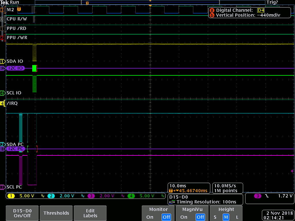 I2C Buffer 2.png [ 25.49 KiB | Viewed 3350 times ]
I made it so that the test itself can drive M2 faster. Also, I really improved the communication between PC and dsPIC -- it now uses a more efficient command structure, which can send multiple commands in 1 message. After this screenshot, I ran the full multiplier test and got all correct answers with this, so that's a good sign that it is working well.
I am still not able to write to the built-in expansion RAM of the MMC5. Here is the code where I attempt to do it:
Code:
private void testFillRam()
{
data_queue = new byte[60];
data_queue_index = 0;
string s = "";
// ** Initialize **
readAndRefreshGraphics();
data_queue[data_queue_index] = 0x03; // Set M2 fast mode
data_queue_index++;
data_queue[data_queue_index] = 0x00; // Set M2 Low
data_queue_index++;
data_queue[data_queue_index] = 0xFF; // Rise CPU R/W
data_queue_index++;
operation_setCpuAddressBusDirection(false); // Set CPU address bus as output.
// Write mode value $02 to register $5102:
operation_setCpuAddress(0x5102);
operation_writeCpuData(0x02);
// Write mode value $01 to register $5103:
operation_setCpuAddress(0x5103);
operation_writeCpuData(0x02);
// Write Extended RAM mode value $02 to register $5104:
operation_setCpuAddress(0x5104);
operation_writeCpuData(0x02);
sendOperationQueueToDsPic();
readResultsFromDsPic(0); // Run the queue.
// ** End Initialize **
// Write non-zero, non-FF, non-negative data to entire expansion RAM:
int i_start = 0x5C00;
int i_end = 0x6000;
byte data_to_write = 0x10;
for (int i = i_start; i < i_end; i++)
{
operation_setCpuAddress((UInt16)i);
operation_writeCpuData(data_to_write);
data_to_write++;
if (data_to_write > 0x7F)
{
data_to_write = 0x10;
}
sendOperationQueueToDsPic();
readResultsFromDsPic(0); // Run the queue.
// Update progress bar in GUI:
SetProgressThreadable(i, i_start, i_end, 100);
}
// Read back entire expansion RAM
i_start = 0x5C00;
i_end = 0x6000;
for (int i = i_start; i < i_end; i++)
{
operation_setCpuAddress((UInt16)i);
operation_readCpuData();
sendOperationQueueToDsPic();
byte[] readback = readResultsFromDsPic(1);
s += i.ToString("X4") + ",";
s += readback[0].ToString("X2") + "\r\n";
SetProgressThreadable(i, i_start, i_end, 100);
}
// Log to File:
filename = "MMC5 Expansion RAM Fill " + DateTime.Now.ToString("MM.dd.yy hh.mm.ss tt");
using (StreamWriter outfile = new StreamWriter(folderName + filename + ".csv", true))
{
outfile.WriteLine(s);
}
SetProgressThreadable(0, 0, 0, 1);
}
Here is the code where I write to registers. It works with the multiplier, but could you guys please verify that I am doing this on this on the correct edge of M2? I am very confused by the edge of M2. I drive the CPU address bus to the intended address right before calling this function.
Code:
private void operation_writeCpuData( byte data )
{
data_queue[data_queue_index] = 0x01; // Set M2 High
data_queue_index++;
data_queue[data_queue_index] = 0xFE; // set CPU R/W low
data_queue_index++;
data_queue[data_queue_index] = 0x56; // Write byte to CPU data bus
data_queue_index++;
data_queue[data_queue_index] = data; // ^ (data)
data_queue_index++;
data_queue[data_queue_index] = 0x66; // Set as output from IO expander to MMC5
data_queue_index++;
data_queue[data_queue_index] = 0x00; // ^ (Output)
data_queue_index++;
data_queue[data_queue_index] = 0x00; // Set M2 Low -- Registers the write on falling edge. (I think???)
data_queue_index++;
data_queue[data_queue_index] = 0x66; // Set as input to IO expander from MMC5
data_queue_index++;
data_queue[data_queue_index] = 0xFF; // ^ (Input)
data_queue_index++;
data_queue[data_queue_index] = 0xFF; // CPU R/W high
data_queue_index++;
}
I always read back all zeros from the internal expansion RAM. Any ideas would be very much appreciated.
Edit:
I tried speeding up M2. Normally, I had a 10msec period on M2 (when idle / waiting for next instruction from PC). I increased the speed to 4msec period and still read all zeros.
The way the NES is "supposed" to work, R/W, all the address lines, and the data lines during a write, should only change while M2 is low. (During a read, you should care about the value of the data bus on the falling edge of M2)
Not clear that's what's going wrong, but it assuredly doesn't help.
Remember that Krzysiobal said that the timeout is 11us, not ms. You may need to have the PIC fake a series of dummy reads to some unrelated address (0 would be good) to speed things up enough.
lidnariq wrote:
Remember that Krzysiobal said that the timeout is 11us, not ms. You may need to have the PIC fake a series of dummy reads to some unrelated address (0 would be good) to speed things up enough.
Oh crap, that's probably the problem. Wow that was a bad mistake, I am thinking this microcontroller thing might have been a complete waste of effort because of that.... I know that I can't update the IO expanders that fast. Will have to rethink this I guess. Not sure, I might want to use a real Nintendo and flash PRG ROM now. That sucks...
Edit:
It takes me at least 74 usec to update an IO expander. I can't control precisely where each byte gets acknowledged and therefore makes it out to the IO expander pins. Deal breaker on that one. But there is always a way. I have these L'Empereurs, I will wire one up with a flashable PRG-ROM. I like
not using the Nintendo because then I am in complete control of everything and I don't miss anything.
Edit 2:
I do have direct control of M2 and CPU R/W. In theory, I could keep M2 trotting along quite fast while setting up data and address busses and set/clear CPU R/W with high precision. But then reads get screwed up because I can't guarantee that the IO expander reads with M2 high. So I would have to make the CPU data bus all direct control too. Possible I guess but not sure I want to commit to invest more into this slow thing just yet. It is great for stuff that doesn't reset - Maybe it keep it as setup A for slow non-normal-NES controlled stuff and work on setup B with a real famicom. Setup B would not have been able to show us exactly how the scanline detection works, for example.
Edit 3:
You know, I don't have the +batt pin hooked up to anything -- I wonder if that is necessary in order to run the internal RAM? I will go back tomorrow and give that a try. Also, I will go ahead and give the hardware timer a try at this slow speed and see what happens.
Edit 4:
The +batt seems doubtful because I measured that pin tonight on a L'Empereur with a dead battery and it did not go up in voltage when run in a Famicom. I would have expected 5V to appear on this pin when running if it were necessary.
What signals do you currently have on the I/O expanders vs the PIC's pins?
You could probably get away with just M2, R/W, D0-D7, /ROMSEL and A14 on the PIC itself, and everything else via the I/O expanders.
I have M2, CPU R/W, PPU /RD and PPU /WR on the Pic right now, everything else on the IO expanders. I do have 29 5V-tolerant pins available on the Pic. I should be able to put all of that and the whole CPU address bus on there. I ended up using a dsPIC33FJ64GS606 which is more RAM but only 64 pins vs the 80-pin '32GS608 that I initially was using. But this 606 micro is known-good, it came from a scrapped board that never got used (it passed blank check when I first rigged it up). It is OK speed, it runs at 40MHz, but most importantly I am very familiar with this particular micro.
I want to probe each unknown pin when turning on and off a 1.79MHz square wave into M2. In case any of them are affected by it, maybe it could have something to do with this reset function. I have not yet definitively seen this reset occur with my own eyes so I am very curious to reproduce it and see what else might be going on -- not that I doubt Krzysiobal. I just have a need to see it and poke at it happening to fully believe it.
I might be able to write to the hardware timer and then immediately start toggling M2 fast and watch /IRQ for example. And then try again with slowing down M2, basically repeating Krzysiobal's test. In addition, I don't think we know that the M2 reset necessarily disables or clears the built-in RAM. I could still be doing something wrong trying to unlock or write or read from it. This would become apparent with "setup B" if I wrote a 6502 program to do this test and put it on flash ROM. I think it is a good idea to have this 2nd setup that runs directly in a Famicom, for reality checks if nothing else.
I tried another 32GS608 today. I want that one because it has has a full 5V tolerant 16-bit port (Port B). I had the same problem with the I2C2 module though -- no acknowledge of the address. I went so far as to start a new project where all it did was set those 2 pins as GPIO outputs and toggle them and THAT didn't work either. We do use these micros where I work, so I might have to make it official to figure out what the heck is going on with that. Unlikely NOT to be my own fault.
I did the test where I put in 1.79MHz into M2 and probed all of the unknown pins. I did find something sort of interesting with the PRG RAM control pins (including unknown pin 75) that might be showing us the exact reset time / behavior.
Quote from before when I also found pin 75 to behave like a PRG RAM pin when looking at voltages with and without pull-down resistor:
Ben Boldt wrote:
- 76 (PRG RAM /WE) 4.96, 3.17
- 72 (PRG RAM 1 /CE), 4.96, 3.17
- 71 (PRG RAM 0 /CE), 4.96, 3.17
- 75 (unknown), 4.96, 3.17
Of particular note: Pin 73 (unknown pin) did not behave this way, it kept its voltage steady with these tests.
Attachment:
File comment: M2 Timeout: 11.24usec
 1. Pin 75, M2 Stop Low, Rise Slowly.png [ 39.8 KiB | Viewed 4165 times ]
Attachment:
File comment: M2 Timeout: 11.59usec
 2. Pin 75, M2 Stop High.png [ 46.08 KiB | Viewed 4165 times ]
Attachment:
File comment: The noise might actually be clocking it here, not sure.
 3. Pin 75, M2 Stop Low.png [ 47.53 KiB | Viewed 4165 times ]
Attachment:
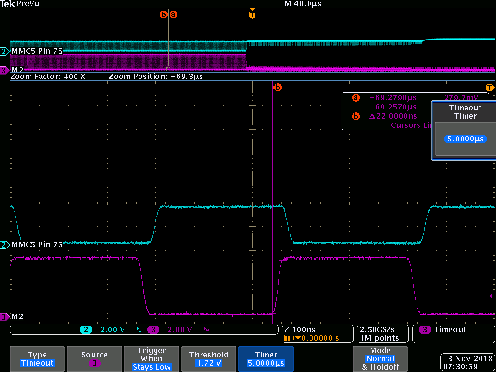 4. Pin 75, inverted + 22nsec delay from M2.png [ 40.06 KiB | Viewed 4165 times ]
Seen here, the timeout can be triggered when M2 is held high for about 11.5 usec, definitely confirming Krzysiobal's findings. It is unknown if the timeout can be triggered with M2 held low.
More attachments, comparison to the other known RAM pins. Very similar!
Attachment:
 5. Pin 76 - PRG RAM !WE.png [ 36.91 KiB | Viewed 4165 times ]
Attachment:
 6. Pin 71 - PRG RAM 0 !CE.png [ 35.98 KiB | Viewed 4165 times ]
Attachment:
 7. Pin 72 - PRG RAM 1 !CE.png [ 40.24 KiB | Viewed 4165 times ]
Edit:
Confirmed M2 held low does trigger reset. Adjusted my scope and setup, new attachment.
Attachment:
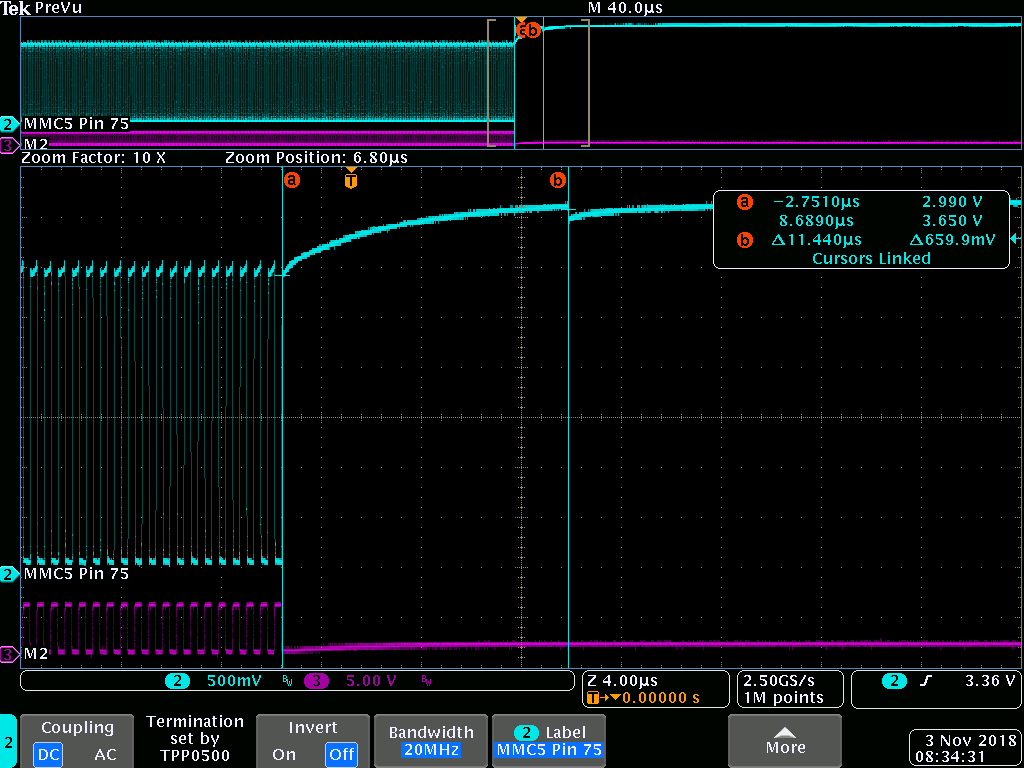 8. Reset with M2 held low confirmed.png [ 42.91 KiB | Viewed 4165 times ]
Edit 2:
Another observation about pin 75. If power is applied to the MMC5 with M2 low, then later M2 starts toggling at 1.79MHz, pin 75 always follows M2, inverted, +22nsec, every time. But if I turn on the 1.79MHz into M2 before applying power, about 3 out of 4 times pin 75 will latch high once power is applied. The latch can always be cleared by stopping M2 and then starting it again.
While latched, if I remove and reapply power many times quickly, with M2 still running the whole time, it stays latched. If I remove power for several seconds and reapply, it is back to the 3 in 4 chance that it will stay latched.
On the wiki, what exactly do you mean by "PRG RAM 2" ?
This pin behaves identically to PRG RAM 1 /CE, so PRG RAM 2 /CE is my best guess. What is on your mind, do you disagree? In my testing, the address bus was $7FFF, RAM /WE always high, RAM 0 /CE always high, RAM 1 /CE was M2 inverted, and pin 75 was also M2 inverted.
It seems like this theory would be enabling 2 RAM chips at the same time. That doesn't really make sense I guess. When I finally get my setup working, I should run through all CPU addresses and watch these pins. For now I will adjust that label in the wiki.
I mean, there are a few possibilities that come to mind...
1- It could be "PRG RAM /CE", for a single 64 KiB SRAM instead of two 32 KiB SRAMs. Another pin should probably be "PRG RAM A15", if so.
2- It could genuinely be "PRG RAM 2 /CE", for a third 32 KiB SRAM. Another pin should probably be "PRG RAM 3 /CE", if so.
Those are just possibilities that are immediately obvious. There might be other options.
Thanks for catching me jumping to conclusions lidnariq -- it is hard to see that happening without a second set of eyes somtimes. I will need to do some more experiments to get a better idea on this.
It was a rough night but I got it running. After figuring out the minimum setup delays before errors started appearing, and then doubling that amount, I have M2 at 50kHz (minimum speed to not trigger reset), and I was able to do the full multiply test with no errors. No I/O expanders were used for this test -- the whole CPU address and data bus is now available directly to the micro.
For the address bus, I used non-5V tolerant pins via this little circuit on each pin:
Code:
10k ohm
|---------+---/\/\/--- 5V
|<--| |
Pic _____|---| +----------- MMC5
|
Gnd
I still have an issue to work on -- If I do attempt to read or write to an I/O expander, the code still pauses M2 for the duration of the transaction. I will have to work on that if I want to be able to use that without causing reset. But for now, I don't think that holds me back from playing with the internal RAM. I will give that a try soon.
I found out more about pin 75 today.
First I made a test that writes $5100 PRG mode. Then for all PRG addresses, when M2 is high it reads back RAM 0 /CE, RAM 1 /CE, and pin 75. In the address range $6000 to $7FFF:
RAM 0: high (inactive)
RAM 1: low (active)
75: low (active)
(outside this range, everything inactive)
Since I never enabled RAM mode in any of the PRG banks, I found this result to be the same for each PRG mode.
Next, I wrote $04 to $5113, which would select RAM chip 1. This had the same result, as expected.
Next, I wrote $00 to $5113, which would select RAM chip 0. In the address range $6000 to $7FFF:
RAM 0: low (active)
RAM 1: high (inactive)
75: low (active)
(outside this range, everything inactive)
Here is my theory on this:
Take L'Empereur for example. It has 2x 8kbyte WRAM, which uses 13 address bits. They could have laid out the board such that there was a 16kbyte WRAM location, with its /CE coming from pin 75, and now using PRG RAM A14. A single ROM could be written such that it keeps bits 1 and 2 the same in $5113. Then the board could be populated with 2x 8k or 1x 16k, whichever is available or cheaper.
It says in the wiki that there is a game that use 1x 32kbyte RAM. Is that right? Where does it get PRG RAM A15 from?
In other news, I was able to write and read back from the internal RAM. I filled it and played with the +$1000 versions of the DMC registers, nothing happened. It definitely could be my setup, but I found that I was able to set read mode in $5010 and I was still able to write raw samples to $5011 and they updated the DAC output. I wrote several values less than $80 to $5010, with and without bit 0 set, and writes to $5011 remained successful. Later on, possibly after a power cycle, I was able to get it into read mode again where it would not allow me to write to $5011. Again -- it might be my setup but I though it was interesting and worth noting.
Edit:
It looks like these 4 Koei games used 32k PRG-RAM:
- Aoki Ookami to Shiroki Mejika: Genchou Hishi
- Nobunaga no Yabou: Bushou Fuuunroku
- Sangokushi II
- Romance of the Three Kingdoms II (i.e. USA version of Sangokushi II)
I always forget about the 0th address bit. 32k makes sense, 2^15 = 32k, 15 address bits is A0 to A14... My bad.
Edit 2:
I should try writing $08 to $5113 and see if it affects pin 75.
Today I tried writing these values to $5113:
None of these had any effect on the range where pin 75 went active. I think I should try setting each bit 7 in registers $5114 - $5117, in each PRG mode in register $5100 and see if 75 shows any different behavior.
So far with what we know, I think a good label for the wiki would be:
71 -> PRG RAM 0 /CE **
72 -> PRG RAM 1 /CE **
75 -> PRG RAM /CE **
** PRG RAM 0 /CE and PRG RAM 1 /CE are selectable by bit 2 in register $5113. This allows the use of 2 PRG-RAM chips. PRG RAM /CE is not affected by bit 2 in register $5113.
1. Yes, I can confirm - pin 75 is just 71 (/PRG0) && 72 (/PRG1). Before knowing that, I wanted to connect single 64K (62512) SRAM to MMC5, which would involve building logic-gate decoder.
Now it can be enabled using just this pin and /PRG0 (or /PRG1) can be used ad A15
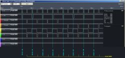
In the example above, pin 73 seems to alter its state around 125ns BEFORE (wtf?) every rising edge of M2. But in fact, it changes its value upon change of address on the addres bus, not the M2, but not does not happens for every address, I need to examine it.
---
pin 73 seems to be 0 when bit $5113.3==0 && CPU address (read/write - no matter) is between $6000-$7fff or $e000-$ffff. It is combinatorial (it changes with CPU address, not with M2)
Spikes on 72/75 at $e000-$ffff are just because of slight delay before M2 and !ROMSEL changes.
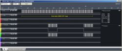
---
pins 81, 82, 92, 29, 30 seems to be input with +5V pullup (voltage drops to 1.3V when shorting with 10k to GND, in contrary to SL3/CL3 where it drops to 0.45V - maybe just pullup is stronger)
pin 93 seems to be output
--
pin 93 drives 0 when bit $5116.2==0 && CPU address is between $4000-$5fff or $c000-$dfff
Very cool stuff krzysiobal, I like what you found with pin 73 and 93, I wonder what that could be used for???
I did some testing today with PRG Mode ($5100) and each PRG bank ($5114,5,6,7). I tried each mode 0-3, and $7F and $FF in each bank register. I did this while monitoring the 3 PRG RAM /CE pins. I never found any place where 75 was not the 'AND' of the other two. Interestingly, though, I found that the RAM got enabled as follows:
Code:
PRG-RAM /CE gets enabled in this extra areas, in addition to $6000-7FFF where it is always enabled:
| Bank 0 7F | Bank 1 7F | Bank 2 7F | Bank 3 7F
--------+-------------+-------------+-------------+-------------
Mode 3 | 8000-9FFF | A000-BFFF | C000-DFFF | none
Mode 2 | 8000-9FFF | A000-BFFF | C000-DFFF | none
Mode 1 | 8000-9FFF | A000-BFFF | C000-DFFF | none
Mode 0 | 8000-9FFF | A000-BFFF | C000-DFFF | none
It seemed to not care about mode. I set my scope to trigger on M2 gap larger than 10.5 usec and it never triggers in this test, so I don't think I am triggering reset. It could be that I am not writing the mode correctly. Any chance you could verify this table? If you get a different result, I probably have more work to do on my setup.
Yes, that's how MMC5 works - if high bit in each of those regs is 0, (value $00-$7F) then RAM in proper region ($8000/$a000/$c000), instead of ROM is enabled.
Okay, well I was confused because the wiki says "ignored" in a lot of areas for registers $5114-5116. I guess this refers only to PRG-ROM. I will edit the wiki to reflect that.
Another question: I have seen PRG-RAM +CE always high in all conditions. What would make this signal go low?
Quote:
Okay, well I was confused because the wiki says "ignored" in a lot of areas for registers $5114-5116. I guess this refers only to PRG-ROM. I will edit the wiki to reflect that.
Well, no, all the rules from Wiki apply. So for example when I wrote
$5100 <- $00
and then
$5114 <- $7f
$5115 <- $7f
$5116 <- $7f
$5117 <- $7f
and then read $8000, no RAM is enabled (I've just tested that on hardware). So in that case $5114-$5116 are ignored.
So your assumption of no dependence on mode register is wrong (maybe there was some bogus write to $5100 that cause the mode to revert back to 3?)
krzysiobal wrote:
Quote:
Okay, well I was confused because the wiki says "ignored" in a lot of areas for registers $5114-5116. I guess this refers only to PRG-ROM. I will edit the wiki to reflect that.
Well, no, all the rules from Wiki apply. So for example when I wrote
$5100 <- $00
and then
$5114 <- $7f
$5115 <- $7f
$5116 <- $7f
$5117 <- $7f
and then read $8000, no RAM is enabled (I've just tested that on hardware). So in that case $5114-$5116 are ignored.
So your assumption of no dependence on mode register is wrong (maybe there was some bogus write to $5100 that cause the mode to revert back to 3?)
Sorry, I misinterpreted. I need to check my setup and revert the wiki....
I have some trouble with setup delays, I suspect the PRG Mode write was not successful due to needing to space things out a little more. In some cases I am most likely exceeding the NES CPU clock by a fair bit.
Quote:
Another question: I have seen PRG-RAM +CE always high in all conditions. What would make this signal go low?
As I observe, +PRG-CE is 1 as long as M2 is cycling (no matter what address is present on bus). Just about 11.2us after the last falling edge of M2, it goes low, so it can be considered as a preview of MMC5's internal /RESET signal
Also, I thought that every register of MMC5 is set to ones on power-up (or during reset).
However, $5114-$5116 seems to be either set to $0 (or just the highest bit is set to 0), because without writing anything to them or to the mode register, RAM seems to be enabled at $8000-$dfff by default.
i was not entirely true abouts pins 73 & 93 - here are full results:
Code:
pin73:
outputs 0 when cpu accesses ($6000-$7fff or $e000-$ffff) and $5113.3=0
outputs 0 when cpu accesses ($0000-$1fff or $8000-$9fff) and $5114.3=0
outputs 0 when cpu accesses ($2000-$3fff or $a000-$bfff) and $5115.3=0
outputs 0 when cpu accesses ($4000-$5fff or $c000-$dfff) and $5116.3=0
otherwise outputs 1
pin93:
outputs 0 when cpu accesses ($6000-$7fff or $e000-$ffff) and $5113.2=0
outputs 0 when cpu accesses ($0000-$1fff or $8000-$9fff) and $5114.2=0
outputs 0 when cpu accesses ($2000-$3fff or $a000-$bfff) and $5115.2=0
outputs 0 when cpu accesses ($4000-$5fff or $c000-$dfff) and $5116.2=0
otherwise outputs 1
I think you found PRG RAM A15 and A16.
Bank register bits:
7 RAM/ROM
6 A19
5 A18
4 A17
3 A16 <- Pin 73 (PRG RAM A16)
2 A15 <- Pin 93 (PRG RAM A15)
1 A14 <- PRG RAM A14
0 A13 <- PRG RAM A13
CPU non-paged address bits:
A0-12 - 8k
Please try the same test with PRG RAM A14 (Pin 70) and see if it reacts the same to bit 1 in $5113/4/5/6.
Code:
I think you found PRG RAM A15 and A16.
Thank you, this is wonderful idea! Glad you could light lamp in my head, cause I firstly thought they are some kind of signals to enable external (additional) memories.
And yes, the sentence from wiki which says that:
Code:
PRG RAM bank ($5113) - select RAM bank for $6000 and $8000/$a000/$c000/$e000
is
WRONGbits 3-0 in $5113/$5114/$5115/$5116 are used to manipulate RAM bank in each regions:
Code:
pin73 (=RAM-A16):
outputs 0 when cpu accesses ($6000-$7fff or $e000-$ffff) and $5113.3=0
outputs 0 when cpu accesses ($0000-$1fff or $8000-$9fff) and $5114.3=0
outputs 0 when cpu accesses ($2000-$3fff or $a000-$bfff) and $5115.3=0
outputs 0 when cpu accesses ($4000-$5fff or $c000-$dfff) and $5116.3=0
otherwise outputs 1
pin93 (=RAM-A15)
outputs 0 when cpu accesses ($6000-$7fff or $e000-$ffff) and $5113.2=0
outputs 0 when cpu accesses ($0000-$1fff or $8000-$9fff) and $5114.2=0
outputs 0 when cpu accesses ($2000-$3fff or $a000-$bfff) and $5115.2=0
outputs 0 when cpu accesses ($4000-$5fff or $c000-$dfff) and $5116.2=0
otherwise outputs 1
pin70 (=RAM-A14)
outputs 0 when cpu accesses ($6000-$7fff or $e000-$ffff) and $5113.1=0
outputs 0 when cpu accesses ($0000-$1fff or $8000-$9fff) and $5114.1=0
outputs 0 when cpu accesses ($2000-$3fff or $a000-$bfff) and $5115.1=0
outputs 0 when cpu accesses ($4000-$5fff or $c000-$dfff) and $5116.1=0
otherwise outputs 1
pin69 (=RAM-A13)
outputs 0 when cpu accesses ($6000-$7fff or $e000-$ffff) and $5113.0=0
outputs 0 when cpu accesses ($0000-$1fff or $8000-$9fff) and $5114.0=0
outputs 0 when cpu accesses ($2000-$3fff or $a000-$bfff) and $5115.0=0
outputs 0 when cpu accesses ($4000-$5fff or $c000-$dfff) and $5116.0=0
otherwise outputs 1
if bit 2 is 0 and bit 7 is 0, them RAM0 is selected (RAM0-!CE is asserted) when accessing corresponding region
if bit 2 is 1 and bit 7 is 0, them RAM1 is selected (RAM1-!CE is asserted) when accessing corresponding region
$5113.7 is always 0 (there is always one of RAMs enabled at $6000)
pin75 (=RAM-!CE = RAM1-!CE && RAM2-!CE)
krzysiobal wrote:
And yes, the sentence from wiki which says that:
Code:
PRG RAM bank ($5113) - select RAM bank for $6000 and $8000/$a000/$c000/$e000
is
WRONGbits 3-0 in $5113/$5114/$5115/$5116 are used to manipulate RAM bank in each regions:
Where do you see that sentense ? For me it has always made sense that each registers bankswitches a specific region / I don't know who came up with the idea that a single register would bankswitch all regions selected on RAM but this probably comes from a misunderstanding.
Probably I misunderstood the sentence:
When selecting a RAM bank, treat bank bits as indicated for the PRG RAM bank register at $5113.
So how would RAM be wired if more than 64k of it were to be present ? Would there be 4 chips, or just one single very large chip ?
a) 1x128K:
RAM.A16 = MMC5.RAM-A16 (73),
RAM.A15 = MMC5.RAM-A15 (93),
RAM.A14 = MMC5.RAM-A14 (70),
RAM.A13 = MMC5.RAM-A13 (69),
RAM.!CS = MMC5.RAM-!CS (75)
b)2x64K
RAM0.A15 = RAM1.A15 = MMC5.RAM-A16 (73),
RAM0.A14 = RAM1.A14 = MMC5.RAM-A14 (70),
RAM0.A13 = RAMA1.A13 = MMC5.RAM-A13 (69),
RAM0.!CS = MMC5-RAM0-!CS (71)
RAM1.!CS = MMC5-RAM1-!CS (72)
I'm not even sure 64k SRAM chips existed - for some reason they liked to skip power of twos, chips were 2k, 8k, 32k or 128k.
(I could be wrong, chips of other sizes might exist but they were probably rarer or more expensive than two chips of the smaller size)
64k exists and I have a few of them (62512, DIL32-3)
I even had quite rare and uncommon 62128 (16k).
Larger (128k, 256k, 512k) also exists (various names), but they are in SO32 package)
BTW. Recently I did subset of MMC5 on FPGA to support Metal Slader Glory translation. I had minor troubles with the screen shaking (this game uses scanline counter two times per frame and it disables PPU rendering also 2 times per frame).
What I've noticed is that there are 4 (not 3) nametable fetches from the same address that appear at beginning of every. No idea why MMC5 just wants 3 sequential fetches as a signal of new scanline.
"at beginning of every" what?
Perhaps the fourth read might be related to the extra dot inserted at the beginning of almost every scanline (except the first line of every other field on NTSC). These are the fetches at the tail end of hblank:
321: BG x=0 tile ID
323: BG x=0 attribute
325: BG x=0 pattern plane 0
327: BG x=0 pattern plane 1
329: BG x=1 tile ID
331: BG x=1 attribute
333: BG x=1 pattern plane 0
335: BG x=1 pattern plane 1
337: BG x=2 tile ID (ignored)
339: BG x=2 tile ID (ignored)
0: BG x=2 tile ID (aborted)
1: BG x=2 tile ID (for real)
3: BG x=2 attribute
5: BG x=2 pattern plane 0
7: BG x=2 pattern plane 1
Could someone show a logic analyzer trace of PPU /RD, PPU A13, and PPU /A13 across an hblank, in order to help characterize this aborted read? I seem to remember reading years ago that it might even differ between NTSC and PAL PPUs.
Would anyone be against this change in the pinout:
75 / -> PRG RAM /CE (R)
72 / -> PRG RAM 1 /CE (R) (RAM/CE | !$5113.2)
71 / -> PRG RAM 0 /CE (R) (RAM/CE | $5113.2)
I base this on my observation of voltage shifts reflecting pin 75 (but still logic high) in the scope shots of 72/71 when disabled via $5113.2. It leads me to believe that the base signal is 75 and the other two have the added combinational logic. I will try to confirm this by measuring propagation delay between 75 and 72/71.
Edit:
This should consider bit 2 in $5113/4/5/6, not just $5113. I think that makes the description too long. Will leave as-is.
Quote:
"at beginning of every" what?
At the beginning of every scanline.
Quote:
Could someone show a logic analyzer trace of PPU /RD, PPU A13, and PPU /A13 across an hblank, in order to help characterize this aborted read? I seem to remember reading years ago that it might even differ between NTSC and PAL PPUs.
Here is from UA6528 (NTSC) - I attach Saleale Logic waveform file. As you can see - near the 'scanline pulse' (generated by FPGA) there are four PPU read cycles with same A13 address (I don't have enough probes to monitor whole A bus at one)
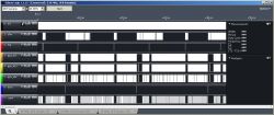
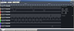

Out of curiosity, when FCEUX is in old PPU mode - there is no single artifacts, when it is in new PPU mode - there are two horizontal bars (as on screenshoot) + two 8x8 pixels artifacts.
On real NTSC hardware, there are just those two 8x8 artifacts.
On Pal hardware the screen acros this gap looks similar to this:

Around 24450 μs, I'm guessing those four read cycles would be
337. x=16 tile number
339. x=16 tile number
1. x=16 tile number
3. x=16 attribute
To confirm this, can you drop one of the CPU signals in favor of PPU A9? If the PPU is rendering the top half of a nametable, A9 indicates whether the PPU is reading a tile number (A9 = 0) or attribute (A9 = 1).
Ok, looks like despite A13 and A12 being same for last four cycles, A9 is only same for three.
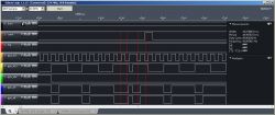
But well, if the sequence to be detected is:
Nametable, Nametable, Nametable, Attribute Table
it is cheaper in terms of resources to just detect if four last fetches have A13=1 (there are no other such fetches per scanline that matches that).
So no idea why MMC5 uses all A0-A13 for comparisions.
BTW. At your post
viewtopic.php?f=9&t=17841&start=135#p228841Shouldn't be there
0: BG x=2 pattern plane 0in place of
0: BG x=2 tile ID (aborted)?
What I also found is that on Dendy (UA6538), idle tick at start of first scaline is present on both odd and even frames.
Do any of you guys have a PAL Nintendo? It would be interesting to compare. I am thinking that the MMC5 would have been designed to work with all different possible PPUs. I have 2 USA front loaders, a dozen Famicoms, and 1 AV Famicom, ALL NTSC unfortunately.
Edit:
Wait a minute, I see you are in Poland krzysiobal, is this a PAL NES you are using?
Ben Boldt wrote:
Do any of you guys have a PAL Nintendo? It would be interesting to compare. I am thinking that the MMC5 would have been designed to work with all different possible PPUs. I have 2 USA front loaders, a dozen Famicoms, and 1 AV Famicom, ALL NTSC unfortunately.
Edit:
Wait a minute, I see you are in Poland krzysiobal, is this a PAL NES you are using?
Correct me if I'm wrong but PAL NES was released mainly in western europe, central europe got famiclones mostly. I have PAL NES but didn't turn it on since years (since NTSC NES is so much superior).
Yea, I have PAL NES, how can I help you?
I am just wondering if the PPU fetches are different for PAL vs. NTSC, possibly to explain why the scanline counter seems more complicated than necessary. Maybe your observation is related to NTSC/PAL too:
Quote:
BTW. At your post viewtopic.php?f=9&t=17841&start=135#p228841
Shouldn't be there
0: BG x=2 pattern plane 0
in place of
0: BG x=2 tile ID (aborted)
?
Would it be helpful for me to do the same testing of the PPU fetches? I know that you have a Just Breed cartridge. Does this mean that you have a genuine Japanese Famicom (NTSC) to go with it? If not, I would be happy to part with one of mine if we can figure out a way to ship it.
Edit:
We can do a little fundraiser for the shipping cost if you want one of my NTSC famicoms krzysiobal. They are all a little yellow but I will pick one out, recap it, do a proper AV mod, and send. You deserve it.
I have a Just Breed cart, NTSC Famicom (but only the new one, not the classic one), and PAL NES. However I didn't understand what you aim to test.
NTSC:
1). Are there those small glitches visible
2) During the screen bellow, is the picture stable or shaking around 1 pixels

[/quote]
PAL:
Are those flawed scanlines visible?
I will work on building a flashable MMC5 cart out of one of my L'Empereurs and give it a try. I waned to make a flashable MMC5 cart anyway, so now I have a good reason. Will install 1MByte PRG and 1MByte CHR. (PLCC32 sockets for 4x AT49F040's) This may take up to 1 week for me to build, heavily influenced by this weekend.
The offer will remain for a freebie NTSC Famicom krzysiobal, you just let me know at any time in the future if you're interested.
Quote:
The offer will remain for a freebie NTSC Famicom krzysiobal, you just let me know at any time in the future if you're interested.
Thank you. My day time job is fixing famicoms/famiclones and similar consoles, so I have tons of them and I'd rather sell them to avoid my shelf collapse rather than acquiring new ones. I am generally testing everything on my home-made one with Dendy/NTSC mode switch, this is more handy than sticking to one console cause of built-in display, possibility to mode select and not-having shell helps adding logic probes.
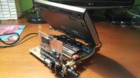
But I would like sincerely thank you for creating this topic and motivating others to validate current state of knowledge. It is really nice to find something new after almost 30 years since first MMC5 left the Nintendo's factory.
BTW. MMC5 has still five unknown pins (inputs) that would be good to investigate. Unfortunatelly reverse engineering inputs its harder. Probably we need to write something like test case for testing every aspect of MMC5 (banking, interrupts, multiplier, nametable switching, split-scree, etc) and then change value of one of those pins and check if some of the behaviour changed.
Hahaha! I should have known you had a million famicoms already. What was I thinking...
I consider this a modern and more advanced way to play Nintendo. I think we are having a lot of fun playing with this, don't you? I have the very distinct advantage of not having any clue what I am doing. I know a bit about microcontrollers but I don't have much prior knowledge of NES mappers, so it gives me a unique perspective vs. you guys.
I made some progress on the flashable MMC5 cart, mechanical is pretty much done at this point:
Attachment:
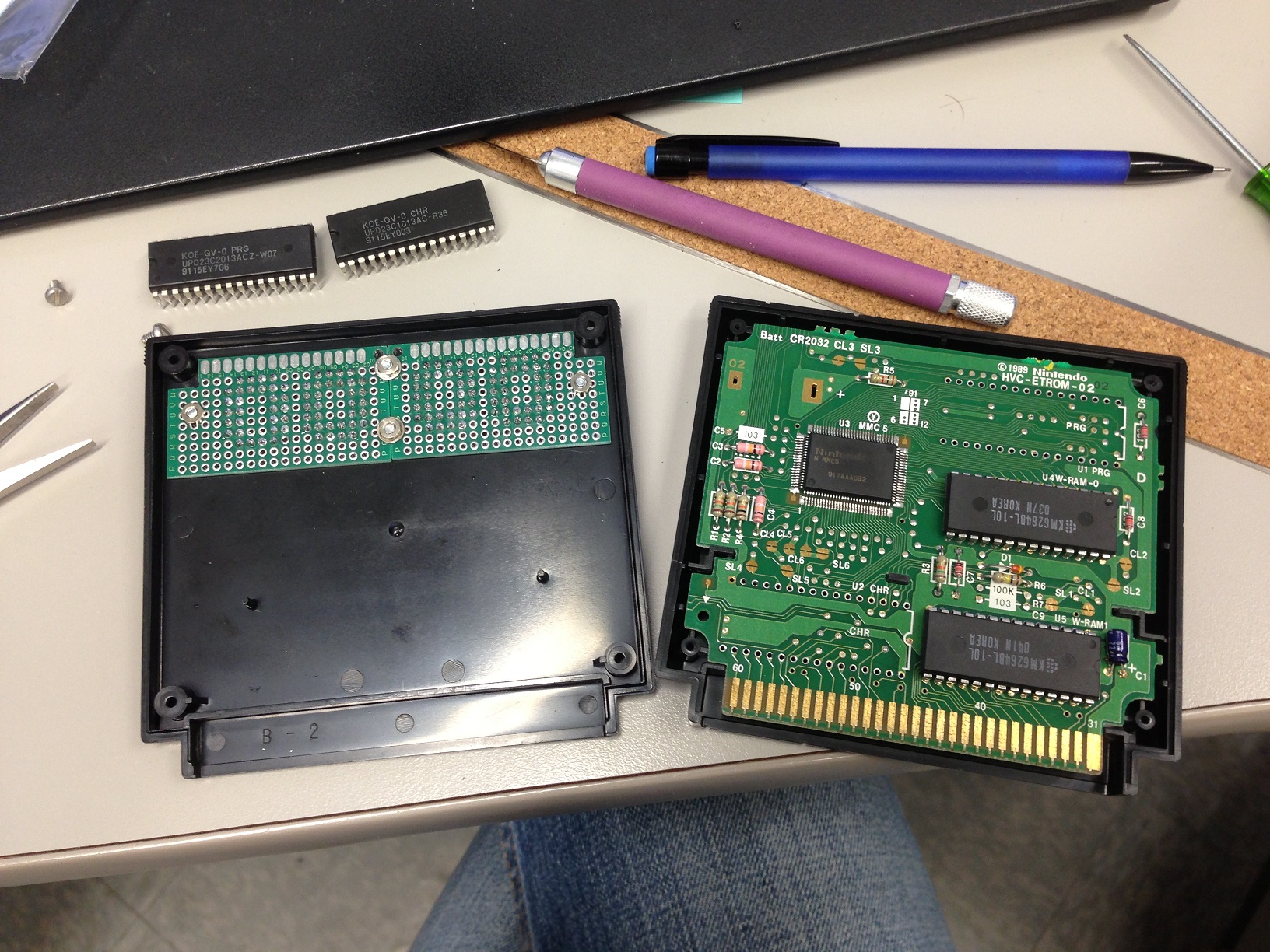 IMG_1581.JPG [ 720.98 KiB | Viewed 4495 times ]
Attachment:
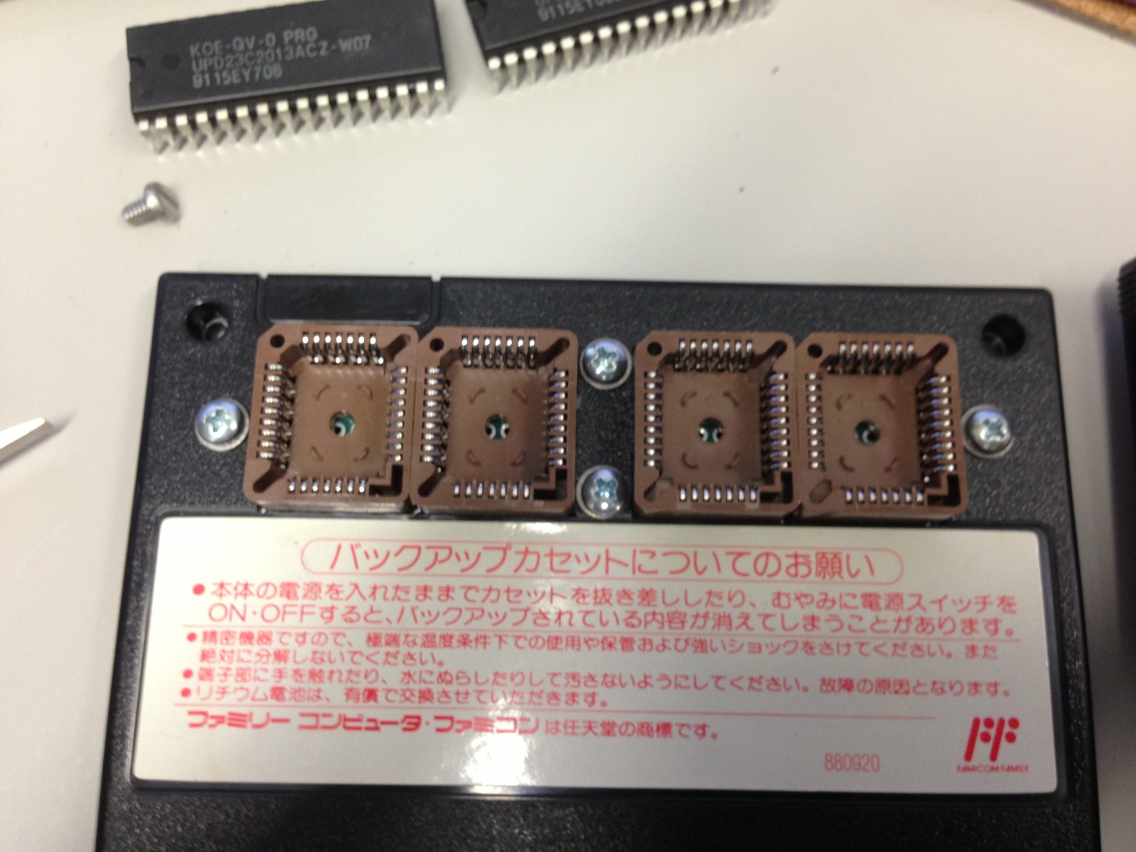 IMG_1582.JPG [ 484.59 KiB | Viewed 4495 times ]
This will support max PRG-ROM and max CHR-ROM. I plan on leaving it with L'Empereur's 2x 8k PRG-RAMs but could modify down the road.
I am building it just like this one:
http://acmlm.kafuka.org/board/thread.php?user=3706Edit:
Next time I order something from Digikey I'll throw a couple of these 128kByte SRAMs in, I can't believe how cheap:
https://www.digikey.com/product-detail/ ... ND/4234576
Quote:
Next time I order something from Digikey I'll throw a couple of these 128kByte SRAMs in, I can't believe how cheap:
https://www.digikey.com/product-detail/ ... ND/4234576Looks like different model (UPD431000ACZ), but with same pinout is available even cheaper in china (US $0.61/piece):
https://www.aliexpress.com/item/D431000 ... b3ae87216bQuote:
You can optimize it by using just one 74*00 in place of 74*00 + 74*04
But it would be even more compact if you 2x 29F080 (+ some adapter) in place of those four ones, that would even fit in the case without need to make extra holes.
Oh nice, I will definitely get those from AliExpress. Thanks for the tip. I have found Aliexpress to be a goldmine for famicom stuff. I even found 2.50mm 72 pin edge connectors there. I think I bought about 10 of them. No more Game Genie sacrifices after that find. I also have a Super Mario Bros. 2J pirate cartridge currently on the way from there, very exciting.
https://www.aliexpress.com/item/item/32805392727.htmlFor the logic gates, I have to use 2x of that whole circuit, one for CHR-ROM and one for PRG-ROM. So either way I have to use 2 chips. This way actually left me with 2 extra 'not' gates in case I ever needed them. I think I used 1 of the inverters for the 62256 RAM chip for some reason having to do with getting the RAM chip into standby mode to prevent excessive battery usage if I remember right. I think I ended up running the whole hex inverter off of the battery in that cart when unpowered.
It was also influenced by what I had in stock. All of my surface mount 74xx chips are recovered from old circuit boards -- I have to be flexible and use what I have somehow or else my "collection" might be considered a hoard!
Then I'd recommend you looking at the datasheet of the memories to check if they are designed for battery retention (and thus low current cosumption).
I was using recently KM62256BLS-7 32K SRAMS (for around 0.6$ in my local shop) and I had very good experience with them - they consumed less than 1uA in standy mode. Unfortunatelly they were no more available so I had to search for something else (I needed something in DIL28-3 package). After a long search I found UM61256FK-15 on aliexpress. They were for 0.3$ so I ordered 100 pieces.
After arrival I tested every single chip and found around 10 to be broken (so it efectively gives 0.33$/piece), but still not bad.
But what was terryfying is that they consume 100uA of current in standby. Which with typical CR2032 3.3V battery wil llast for 3months.
And when I touch its legs, the consumption is not steady and rises to even 400uA. Probably the first ones have pullups on address lines that are enabled when entering standby.
Presence of letter L in the name suggests optimization for low-current uses.
Maybe this one (HM628512LP-5 - $ 1.98 / piece ) is better. Though it is 512 kB instead of 128 kB
https://www.aliexpress.com/item/5pcs-lo ... 2430ee5e90Quote:
I also have a Super Mario Bros. 2J pirate cartridge currently on the way from there, very exciting.
https://www.aliexpress.com/item/item/32805392727.htmlI am curious how the cartridge looks inside. What I can say for sure is that the shells for those (not the ones around 2 centimeters shorter) are quite good quiality.
I don't remember now exactly what happened but I had to hold /CS high with the cart off or something and the mapper chip didn't hold that signal high. Something like that. Not completely sure it was the MMC5 cart either TBH. The RAM chip was HM62256BLP-7, which I recall being several dollars each. I love this bargain you found, I plan to take a chance on 5 of the 128k. The bigger ones you linked to are a little bigger risk having 0 orders and 0 reviews.
Someone from Russia ordered one of the SMB2J carts and posted a picture of the inside in his review:
Attachment:
 inside smb2j.jpg [ 131.38 KiB | Viewed 4809 times ]
Sort of interesting these days to see the ROMs and RAM as DIPs. I suspect the mapper is that glob between the ROMs.
Here are the 2.50mm 72-pin edge connectors (top-load / Game Genie type, not ZIF):
https://www.aliexpress.com/item/item/32827561164.htmlThis is from Aliexpress store Kingworld, I have ordered loads of parts from them. They are great. One time they goofed up an order (missing some things that I ordered). They fixed it.
Overall I have very mixed success on AliExpress. I would say that about 1 in 20 orders goes wrong. I have ordered "new" chips that were obviously scavenged on a way-too-hot solder pot and didn't work on top of that... So you never know. I tend to rely on number of orders and reviews, but also willing to take a chance and be the first reviewer. If ever you get screwed and open a dispute, my advice, never apply for a full refund. AliExpress will decide that you need to send it back and wait for you to provide a tracking number, and if you don't, no refund, done deal. Always leave at least 1 cent not requested in your refund. I am a big fan of AliExpress though. I get all sorts of junk there, flashlights, burning lasers, sunglasses, zip ties, parts for my bicycle, fidget spinners (still addicted), basically any lightweight made in China junk.
Quote:
Overall I have very mixed success on AliExpress. I would say that about 1 in 20 orders goes wrong. I have ordered "new" chips that were obviously scavenged on a way-too-hot solder pot and didn't work on top of that... So you never know. I tend to rely on number of orders and reviews, but also willing to take a chance and be the first reviewer. If ever you get screwed and open a dispute, my advice, never apply for a full refund.
Luckiliy I demanded full return only few times (in all cases the item has not been delievered).
But from my experience I can say that there are few kinds of items you can get:
* Original chips (no idea where they got them, probably the factories that make original chips for for example Altera sell them chips not meeting 100% requirements).
* Some old savaged stuff (for example I bought one time HM62512 SO32 SRAMS that had curved legs, all of them were stored lose, or CPU/PPU for Famicom - those looks like brand new, the legs did not have markings of solder, but around 20% of them were not working)
* Some refubrished stuff - they paint old chips with new markings (I bought one time TSOP48 29LV640 memories, which had.. pin 1 dot painted on the wrong side
I think this presentation shows greatly how China integrated circuit business works
http://asq.org/asd/2009/03/compliance/c ... -parts.pdfQuote:
Someone from Russia ordered one of the SMB2J carts and posted a picture of the inside in his review:
This PCB indeed looks like it was made by some russian hackers, here is link to their site with other similar cartridges, also built-in using old DIP chips, but with new PCBs:
https://vk.com/retronicaruAs I can recall, there is SMB2J hack ported to MMC4 so no big deal.
I have been to China for work before, I can't say I'm surprised by those photos. More wishing I could happen upon some of those heaps of parts for sale!
I think for hobbyist purposes, where is the harm. Most of my junk used to be in something else already anyway, I just do it on a smaller scale. But if a business thought they were buying legit parts and got those, I see where that is a bad deal. That is a really big difference.
I was looking into building an SMB2J cart, but the ROM file I had was some strange mapper. I sort of gave up on it. So just for the purpose of having that game on a cart is mostly what I am sort of after. I wouldn't be against trying to dump it either though just for curiosity. I have heard that often times SMB2J ROM conversions are lacking a wind effect, it will be interesting to see if that works or not in this cartridge.
No new progress on the MMC5 cart build. Will see what I can do this weekend on it.
Today's progress, CHR-ROM is done except for /CE and A19 logic. It looks like PRG-ROM only uses 1 /CE, so I can probably directly use A19 (and /A19) for the other /CE.
Attachment:
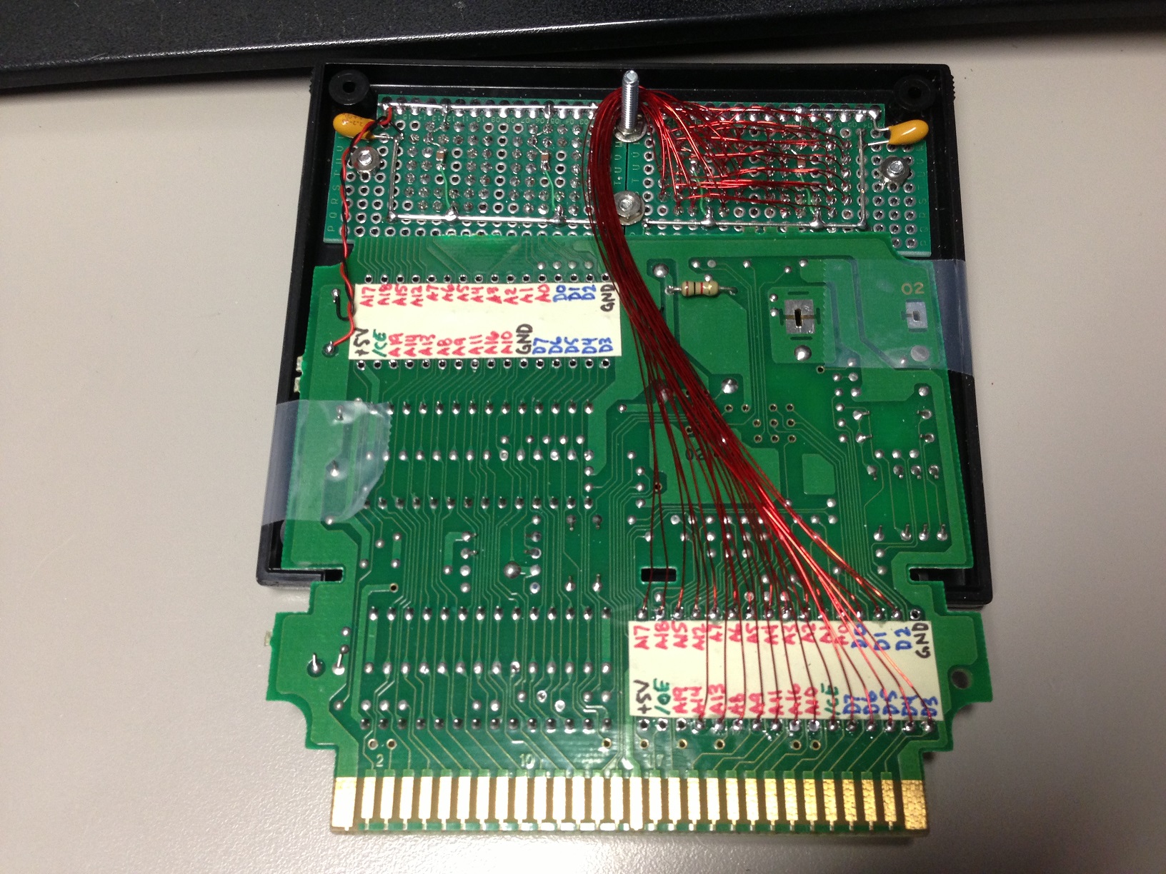 chr-rom.jpg [ 670.21 KiB | Viewed 4752 times ]
It is all wired now. When I get home tonight, I will burn some ROMs and try it. Wish me luck!
Note: I did tie the inputs of the extra NANDs to GND after this photo.
Attachment:
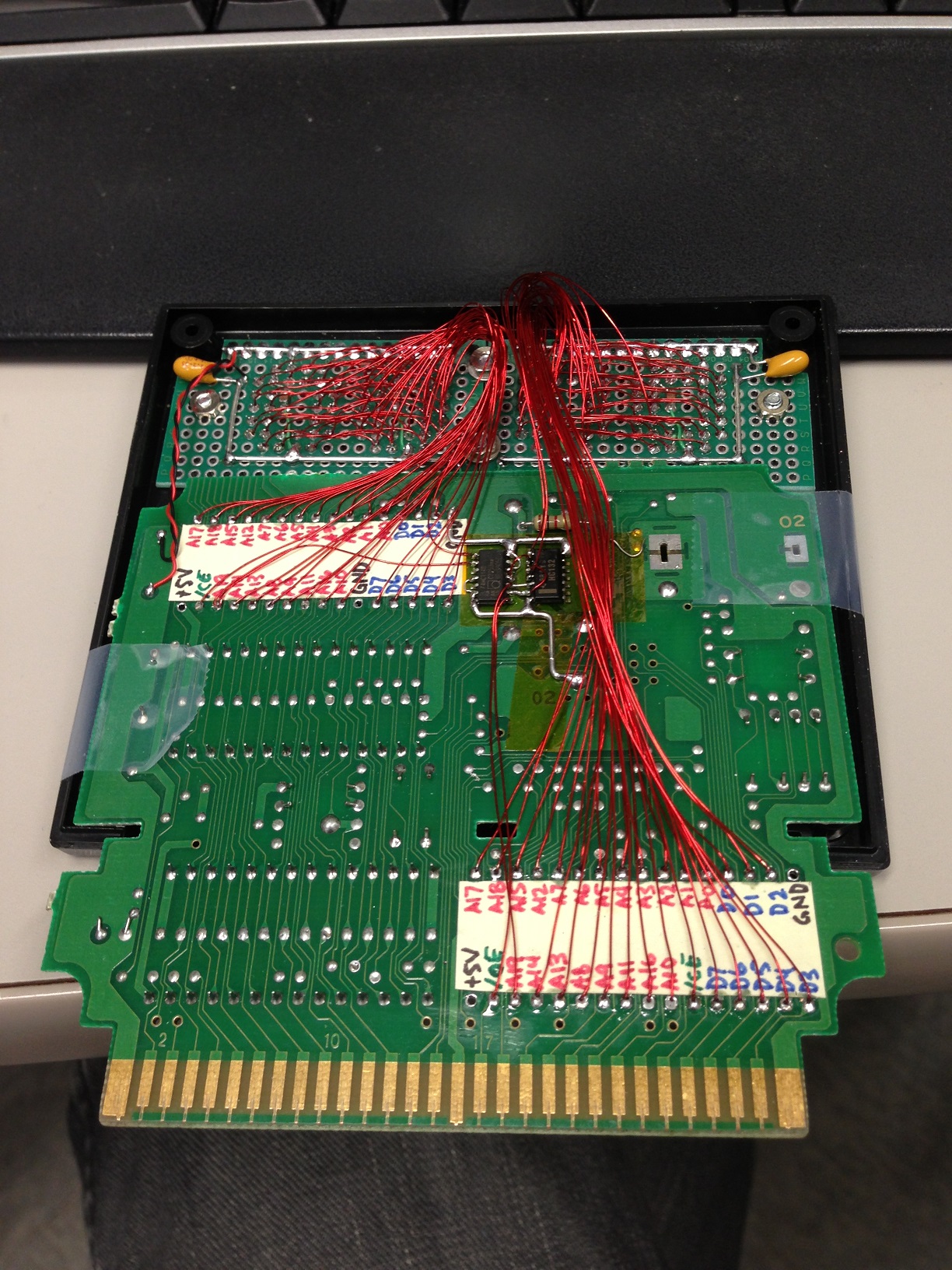 IMG_1584.JPG [ 697.47 KiB | Viewed 4699 times ]
Closed:
Attachment:
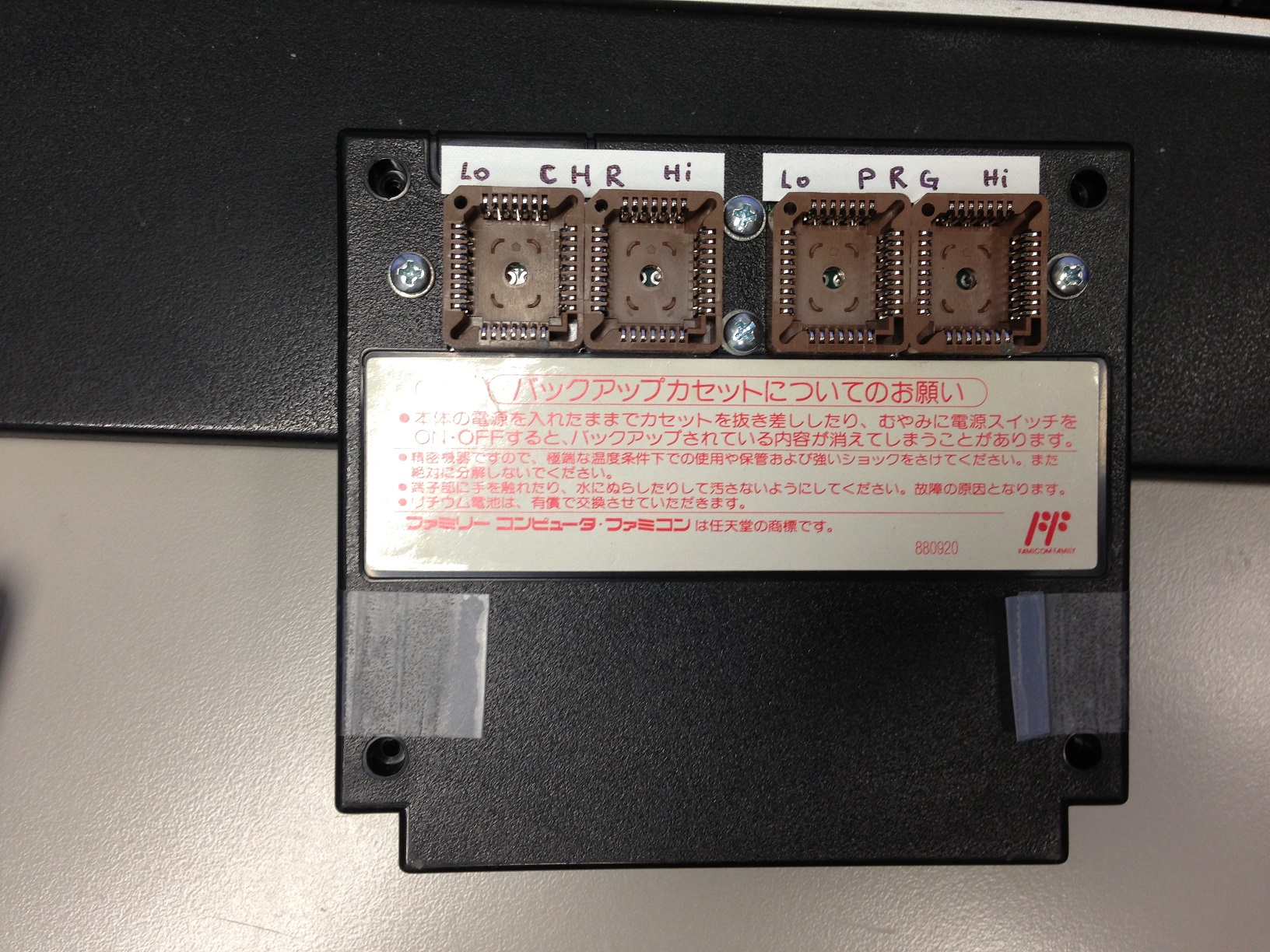 IMG_1585.JPG [ 720.2 KiB | Viewed 4699 times ]
Edit:
Success! No problems!
Here it is running on a Famicom:
https://youtu.be/-B6YsU2MyHwHere it is running on my Hi-Def NES front-loader:
https://youtu.be/S0E5zq3l_kg
Now that we know the answers to your questions about glitches and shaking do exist on NTSC in a cart krzysiobal, I tried an experiment with Just Breed in this cartridge. I burned a ROM with all writes to $5800 replaced by NOPs. I played the game a fair ways, all the way to the next town with the wizard and I found no particular difference. I then burned another ROM with only the write of $00 to $5800 replaced by NOPs. Again, no difference found. At no point did I see any graphics that would have used scanline counting though, not sure if this game ever does that or not.
I decided to lay out all know addresses of the MMC5 address range $5000 - $5FFF visually to look for patterns. I noticed that $5800 is offset back from the expansion RAM by exactly the size of an additional expansion RAM. Also it seems very odd that registers $5110,11,12 are skipped. In addition, the register just before CL3/SL3 status ($5207): oddly skipped as well. These are some open mysteries worth thinking about/investigating.
Code:
$5000 -+-------------------------------------------------+----------------
| Audio Registers | vv 1st Quarter
$5120 -+-------------------------------------------------+
| |
| (unused) |
| |
$5100 -+-------------------------------------------------+
| PRG Banking Mode Registers |
$5110 -+-------------------------------------------------+
| PRG Bank Select Registers, skipping $5110,11,12 |
$5120 -+-------------------------------------------------+
| CHR Banking Mode Registers |
$5130 -+-------------------------------------------------+
| CHR Bank Select Register |
$5140 -+-------------------------------------------------+
| |
| (unused) |
| |
$5200 -+-------------------------------------------------+
| Vertical Split Mode, Multiplier, Hardware Timer |
$5210 -+-------------------------------------------------+
| |
| |
| (unused) |
| |
| | ^^ 1st Quarter
$5400 -+-------------------------------------------------+----------------
| | vv 2nd Quarter
| |
| |
| |
| |
| (unused) |
| |
| |
| |
| |
| |
| | ^^ 2nd Quarter
$5800 -+-------------------------------------------------+----------------
| Just Breed writes to $5800 each v-blank. | vv 3rd Quarter
| |
| |
| |
| |
| Note: Section $5800 - $5BFF |
| Same size as expansion RAM. |
| |
| |
| |
| |
| | ^^ 3rd Quarter
$5C00 -+-------------------------------------------------+----------------
| | vv 4th Quarter
| |
| |
| |
| |
| Expansion RAM |
| |
| |
| |
| |
| |
| | ^^ 4th Quarter
$6000 -+-------------------------------------------------+----------------
Edit:
Another experiment, I inverted all 3 values written to $5800 in Just Breed and tried it in the cart. Still no difference found.
Edit 2:
Referring to what definitely appears to be Nintendo's patent on the MMC5 DAC:
https://patents.google.com/patent/US5317714?oq=5317714This makes it look very discouraging that there would be a way for the MMC5 to play audio directly out of its own RAM. Though it talks very specifically about DAC read mode and write mode, no function having to do with automatic playing from its own RAM is ever mentioned sadly. But coming to save the day with a bit of humor, "The analog sound source circuit 11a [referring to the sound generators in the 2A03] comprises four types of sound generators for generating two types of square waves, a triangular wave
and a sine wave." LOL.
Back to $5800:
We could suppose that the $5800 stuff was for debug or was left in there developing with an earlier version of the MMC5. Things like that could explain it away. That is so strange to have half of the address space in the center go unused though, or used just only for 1 seemingly pointless register right exactly smack in the very center. It seems reasonable that they would have used half of the total space:
$5000
Registers
$5400
Expansion RAM
$5800
or
$5800
Registers
$5C00
Expansion RAM
$6000
Too strange for me, I have a feeling there is something there. It could be write-only RAM (for what purpose, who knows) or enabled somehow by $5104 or $5108 - 5112... I need to fix my setup so I can reliably write to PRG mode registers and see if I can do anything to get some data bus action when reading in $5400-5BFF.
Looking graphically at the PRG banking registers, pretty sure I found a pattern to explain away the missing $5110/11/12:
Code:
+------+----------++-------------+-----------+-----------+-----------+
| Bank | Register || Mode 3 | Mode 2 | Mode 1 | Mode 0 |
+------+----------++-------------+-----------+-----------+-----------+
| [0] | [5110] || [0000-1FFF] | [X] | [X] | [X] |
| [1] | [5111] || [2000-3FFF] | [X] | [X] | [X] |
| [2] | [5112] || [4000-5FFF] | [X] | [X] | [X] |
| 3 | 5113 || 6000-7FFF | ? | ? | ? |
| 4 | 5114 || 8000-9FFF | v[5115] | v[5115] | v[5117] |
| 5 | 5115 || A000-BFFF | 8000-BFFF | 8000-BFFF | v[5117] |
| 6 | 5116 || C000-DFFF | C000-DFFF | v[5117] | v[5117] |
| 7 | 5117 || E000-FFFF | E000-FFFF | C000-FFFF | 8000-FFFF |
+------+----------++-------------+-----------+-----------+-----------+
It would be interesting to see if the MMC5 PRG output address bits reflect $5110/11/12 even though /CS would be disabled. Also, special attention to $5112 for experiments with accessing possibly mysterious RAM at $5800. Also, I am not sure if anyone has ever checked $5113 behavior versus PRG mode.
Edit:
I have a question for you guys that may have a very obvious answer, I feel embarrassed to ask. Why are there separate address pins for PRG-RAM versus PRG-ROM? For example, why is there a PRG A13 pin and also a separate PRG-RAM A13 pin? How and in what conditions would those ever need to be different than each other?
Ben Boldt wrote:
It would be interesting to see if the MMC5 PRG output address bits reflect $5110/11/12 even though /CS would be disabled.
[...]
Why are there separate address pins for PRG-RAM versus PRG-ROM? For example, why is there a PRG A13 pin and also a separate PRG-RAM A13 pin? How and in what conditions would those ever need to be different than each other?
These are actually the same question: The MMC5 actually has two 4-way multiplexers instead. This means they don't have to detect whether it's a write to $6000 or to $E000, so can avoid the problem with setup times on the RAM's address bus. The other option (for use with a single 8-way multiplexer) would need a lot more delay before /RAMCE goes true.
I had not thought about setup delays, that is very intriguing and I had a VERY hard time grasping what you said. I am still not quite sure I get it. Maybe it is easier for me to explain the way I understand and you can correct errors or fill in gaps.
No matter what, CPU A0 - A12 is always connected directly to PRG-RAM and ROM. Those are out of the picture.
PRG A13+ are set by PRG bank registers. I was stuck here -- it seems when you write to a bank register, those A13+ just stay set until you change them again, so I was thinking that it took at least a couple cycles to fetch an LDA $6000 instruction for example, plenty of setup time on A13+. It occurred to me that there are indeed separate PRG banks and when you cross the boundary from one bank into another, the A13+ need to update to that other bank super speedy. So in that case, I definitely see where setup delays are a big deal.
I guess I still don't understand how that would be different for RAM and ROM, why not just use the super speedy ones intended for RAM for ROM too? Sorry I think I just don't get it still.
PRG-RAM-A are dependent only on:
* CPU-A14/A13,
* The value stored at bank register, let's call them: $5113.0-3, $5114.0-3, $5115.0-3, $5116.0-3
* Current PRG-mode (let's call them $5100.0-1)
Because when in 16K mode, lowest bit of bank register is ignored, input-output dependence looks like:
PRG-RAM-A13 = f(CPU-A14, CPU-A13, $5113.0, $5114.0, $5115.0, $5116.0, $5100.0, $5100.1)
PRG-RAM-A14 = f(CPU-A14, CPU-A13, $5113.1, $5114.1, $5115.1, $5116.1, $5100.0, $5100.1)
PRG-RAM-A15 = f(CPU-A14, CPU-A13, $5113.2, $5114.2, $5115.2, $5116.2, $5100.0, $5100.1)
PRG-RAM-A16 = f(CPU-A14, CPU-A13, $5113.3, $5114.3, $5115.3, $5116.3, $5100.0, $5100.1)
If they wanted to make just single PRG-A13 (that would combine both PRG-RAM-A13 and PRG-ROM-A13), the decoder would also need to take into account M2 and CPU_!ROMSEL, cause assess to $E000-$FFFF and $6000-$7FFF is indistinguishable without them
So
PRG-A13 would be f(CPU-A14, CPU-A13, M2, CPU_!ROMSEL, $5113.0, $5114.0, $5115.0, $5116.0, $5117.0, $5100.0, $5100.1))
And same for PRG-A14-A16, so it would probably cost more resources and that's why separating those pins.
Now as I suspect (I havent't tested that yet)
PRG-ROM-A13 is just f(CPU-A14, CPU-A13, $5114.1, $5115.1, $5116.1, $517.1, $5100.0, $5100.1)
I don't think it is a problem of the delay between !ROMSEL and M2 change, cause:
* MMC5 does not have write registers at $E000-FFFF
* logic for decoding PRG-!CE / WRAM-!CE is already responsible for that
krzysiobal wrote:
If they wanted to make just single PRG-A13 (that would combine both PRG-RAM-A13 and PRG-ROM-A13), the decoder would also need to take into account M2 and CPU_!ROMSEL, cause assess to $E000-$FFFF and $6000-$7FFF is indistinguishable without them
I thought that M2 and /ROMSEL would only be considered in PRG/CE and PRG RAM/CE, I guess I don't see how this would be a factor in the address bits. With $E000 vs. $6000, aren't all the address bits out there to the ROMs and RAMs the same and then the /CE's make the choice?
But $5113 is for $6000-$7fff and $5117 is for $e000-$fff so if u won't take !ROMSEL/M2 into account, how u will know which one of those regs to use?
Ben Boldt wrote:
With $E000 vs. $6000, aren't all the address bits out there to the ROMs and RAMs the same and then the /CE's make the choice?
Only because there are two independent multiplexers. Otherwise, the bankswitching hardware would have to detect whether A15 was high or low, and delay the /CEs until after it had determined which it was.
krzysiobal wrote:
But $5113 is for $6000-$7fff and $5117 is for $e000-$fff so if u won't take !ROMSEL/M2 into account, how u will know which one of those regs to use?
OHHHHH I get it now, thanks!
lidnariq wrote:
Ben Boldt wrote:
With $E000 vs. $6000, aren't all the address bits out there to the ROMs and RAMs the same and then the /CE's make the choice?
Only because there are two independent multiplexers. Otherwise, the bankswitching hardware would have to detect whether A15 was high or low, and delay the /CEs until after it had determined which it was.
Man you guys are smart, I don't know if I would have ever figured that out.
What is going on with that table `Bank register effective CPU address ranges versus PRG mode` because I don't get it (I mean the $5110/$5111/$5112 rows + the "covered" comment).
Have you tested that value written to $5110/$5111/$5112 is present on PRG-ROM-A bus for some CPU-A address?
Because I think this table is not true. If we want to make such detailed descriptions (like what address is outputted by MMC5 when accessing certain memory regions), then I think the table should look like that (for PRG_RAM_A - all rows are tested, for PRG_ROM_A it is not tested but the rows below $8000 are in my opinion just mirrors)
Code:
$0000 $2000 $4000 $6000 $8000 $a000 $c000 $e000
-- Mode 0 ---------------------------------------------------------------------------------
PRG_RAM_A | $5113 | $5113 | $5113 | $5113 | $5113 | $5113 | $5113 | $5113 |
PRG_ROM_A | <<$5117>> | <<$5117>> |
PRG | - | - | - | RAM | ROM |
-- Mode 1 ---------------------------------------------------------------------------------
PRG_RAM_A <$5115> | $5113 | $5113 | <$5115> | $5113 | $5113 |
PRG_ROM_A | <$5115> | <$5117> | <$5115> | <$5117> |
PRG | - | - | - | RAM | $5115.7 | ROM |
-- Mode 2 ---------------------------------------------------------------------------------
PRG_RAM_A | <$5115> | $5116 | $5113 | <$5115> | $5116 | $5113 |
PRG_ROM_A <$5115> | $5116 | $5117 | <$5115> | $5116 | $5117 |
PRG | - | - | - | RAM | $5115.7 | $5116.7 | ROM |
-- Mode 3 ---------------------------------------------------------------------------------
PRG_RAM_A | $5114 | $5115 | $5116 | $5113 | $5114 | $5115 | $5116 | $5113 |
PRG_ROM_A | $5114 | $5115 | $5116 | $5117 | $5114 | $5115 | $5116 | $5117 |
PRG | - | - | - | RAM | $5114.7 | $5115.7 | $5116.7 | ROM |
< > = ignore bottom bit (replace it with CPU_A13)
<< >> = ignore two bottom bits (replace bit 1 with CPU_A14 and bit 0 with CPU_A13)
krzysiobal wrote:
What is going on with that table `Bank register effective CPU address ranges versus PRG mode` because I don't get it (I mean the $5110/$5111/$5112 rows + the "covered" comment).
Have you tested that value written to $5110/$5111/$5112 is present on PRG-ROM-A bus for some CPU-A address?
I definitely have
not tested my table yet, and it is very possible that it is incorrect. To indicate this, I left the following message:
Quote:
PRG Bank 0, 1, 2 ($5110-5112)
These registers have no known effect because they presumably point to areas outside of PRG program space.
When I am finally able to work on my setup and get PRG mode writes working correctly, I will test thoroughly and with your help, interpret the results.
I think that the main difference in my table versus your table is that I ignore any ranges where /CS would not be enabled. I think your table is considering strictly the PRG A13+ and PRG-RAM A13+ even in cases where /CS is disabled.
I consider mode 3 to be the "natural" state. We have known this information for a fact previously:
Mode 3 CPU Address Ranges affected:
$5110 n/a
$5111 n/a
$5112 n/a
$5113 -> $6000-7FFF
$5114 -> $8000-9FFF
$5115 -> $A000-BFFF
$5116 -> $C000-DFFF
$5117 -> $E000-FFFF
The pattern I observed is that each PRG bank register in mode 3 covers a complimentary range of $2000 bytes of CPU address space. My extrapolation was this, which seemed pretty reasonable to me:
Mode 3 CPU Address Ranges affected:
$5110 ->
$0000-1FFF, though all /CS's would be disabled in this range
$5111 ->
$2000-3FFF, though all /CS's would be disabled in this range
$5112 ->
$4000-5FFF, though all /CS's would be disabled in this range
$5113 -> $6000-7FFF
$5114 -> $8000-9FFF
$5115 -> $A000-BFFF
$5116 -> $C000-DFFF
$5117 -> $E000-FFFF
Moving on to Mode 2 here is what we already knew:
$5110 n/a
$5111 n/a
$5112 n/a
$5113 -> $6000-7FFF (?)
$5114 -> $8000-
BFFF
$5115 -> n/a
$5116 -> $C000-DFFF
$5117 -> $E000-FFFF
Looking at Mode 2 alongside Mode 3:
reg -> mode 3 -> mode 2
$5110 -> $0000-1FFF -> ?
$5111 -> $2000-3FFF -> ?
$5112 -> $4000-5FFF -> ?
$5113 -> $6000-7FFF -> $6000-7FFF (?)
$5114 -> $8000-9FFF -> $8000-
BFFF
$5115 -> $A000-BFFF -> n/a
$5116 -> $C000-DFFF -> $C000-DFFF
$5117 -> $E000-FFFF -> $E000-FFFF
We can see that in mode 2, $5115 has no effect due to its "natural mode 3 range" being covered by $5114. that is what I meant by "covered by".
I made the same type of extrapolations going to mode 1 and mode 0.
The MMC5 wiki page states that it is not yet known how the MMC5 detects the sprite size (8x8 vs. 8x16) to determine whether to use the $5128-$512B registers. Any news on that front?
There is absolutely no reason to think that there's a physical register mapped at $5110 through $5112. As we stated earlier, because there are two separate address buses for RAM and ROM, the outputs for both bankswitching address buses should completely ignore A15.
I guess I didn't mean to specifically imply that those registers "exist", I have placed them there more to show the offset to register $5113 and why it would have skipped them. Definitely we have seen no known effect from those registers and I have not tested and found any indication of their existence myself.
I think again I have jumped the gun changing the Wiki. I have a very different way of thinking on some of these things that in some cases (this one likely included) is not always right. My mistake is updating the wiki before having enough discussion. Sorry about that. It is just too tempting sometimes. But we will get it sorted and soon the wiki will be accurate again as we continue to investigate and update. That is kind of the benefit and drawback of Wiki is that it is never really a "final" version... In a way, we are brainstorming here, and we must remember that bad ideas can turn into good ideas if we give it a chance and think about it.
It seems that krzysiobal's table works in the reverse perspective of mine. Here is my interpretation of a table built in that way:
Code:
$0000 $2000 $4000 $6000 $8000 $a000 $c000 $e000
-- Mode 3 ---------------------------------------------------------------------------------
PRG_RAM_A | n/a | n/a | n/a | $5113 | $5114 | $5115 | $5116 | n/a |
PRG_ROM_A | n/a | n/a | n/a | n/a | $5114 | $5115 | $5116 | $5117 |
PRG | - | - | - | RAM | $5114.7 | $5115.7 | $5116.7 | ROM |
-- Mode 2 ---------------------------------------------------------------------------------
PRG_RAM_A | n/a | n/a | n/a | $5113 | <$5115> | $5116 | n/a |
PRG_ROM_A | n/a | n/a | n/a | n/a | <$5115> | $5116 | $5117 |
PRG | - | - | - | RAM | $5115.7 | $5116.7 | ROM |
-- Mode 1 ---------------------------------------------------------------------------------
PRG_RAM_A | n/a | n/a | n/a | $5113 | <$5115> | n/a |
PRG_ROM_A | n/a | n/a | n/a | n/a | <$5115> | <$5117> |
PRG | - | - | - | RAM | $5115.7 | ROM |
-- Mode 0 ---------------------------------------------------------------------------------
PRG_RAM_A | n/a | n/a | n/a | $5113 | n/a |
PRG_ROM_A | n/a | n/a | n/a | n/a | <<$5117>> |
PRG | - | - | - | RAM | ROM |
< > = ignore bottom bit (replace it with CPU_A13)
<< >> = ignore two bottom bits (replace bit 1 with CPU_A14 and bit 0 with CPU_A13)
NewRisingSun wrote:
The MMC5 wiki page states that it is not yet known how the MMC5 detects the sprite size (8x8 vs. 8x16) to determine whether to use the $5128-$512B registers. Any news on that front?
I don't think we have looked at that yet NewRisingSun but it may be a future topic to investigate as we get through some of this PRG stuff.
lidnariq wrote:
the outputs for both bankswitching address buses should completely ignore A15.
If this is true, why not combine registers $5113 and $5117 and use the RAM/ROM bit?
Edit:
Answer: Because both ram and rom are enabled at the same time with independent PRG banks because of that.
I'd say what's going on looks something like this:
Code:
$0000 $2000 $4000 $6000
or $8000 $a000 $c000 $e000
-- Mode 3 -----------------------------------------
PRG_RAM_A | $5114 | $5115 | $5116 | $5113 |
PRG_ROM_A | $5114 | $5115 | $5116 | $5117 |
-- Mode 2 -----------------------------------------
PRG_RAM_A | <$5115> | $5116 | $5113 |
PRG_ROM_A | <$5115> | $5116 | $5117 |
-- Mode 1 -----------------------------------------
PRG_RAM_A | <$5115> | ??? | $5113 |
PRG_ROM_A | <$5115> | <$5117> |
-- Mode 0 -----------------------------------------
PRG_RAM_A | ??? | ??? | ??? | $5113 |
PRG_ROM_A | <<$5117>> |
The ???s are both unknown and due to how the chip enables work, can't be made relevant without a custom PCB. But I'd hunch that in the $8000-$DFFF range, PRG_RAM_A and PRG_ROM_A are the same value.
Quote:
If this is true, why not combine registers $5113 and $5117 and use the RAM/ROM bit?
Answer: Because both ram and rom are enabled at the same time with independent pages because of that.
Bingo.
I completely agree with your table, it makes perfect sense and definitely covers all scenarios where the ROM or RAM can be enabled.
Though it won't make a functional difference, I can't feel satisfied that they wouldn't have done it like this, and this is what has been making me feel itchy about this:
Code:
$0000 $2000 $4000 $6000
or $8000 $a000 $c000 $e000
-- Mode 3 -----------------------------------------
PRG_RAM_A | $5110 | $5111 | $5112 | $5117 |
PRG_ROM_A | $5110 | $5111 | $5112 | $5113 |
-- Mode 2 -----------------------------------------
PRG_RAM_A | <$5111> | $5112 | $5117 |
PRG_ROM_A | <$5111> | $5112 | $5113 |
-- Mode 1 -----------------------------------------
PRG_RAM_A | <$5111> | ??? | $5117 |
PRG_ROM_A | <$5111> | <$5113> |
-- Mode 0 -----------------------------------------
PRG_RAM_A | ??? | ??? | ??? | $5117 |
PRG_ROM_A | <<$5113>> |
Edit:
It may be a trivial exercise but when I am able to set PRG mode, I think I will test and confirm 4 separate charts:
- PRG Mode vs. CPU address - which register it gets PRG A13-19 from
- PRG Mode vs. CPU address - which register it gets PRG /CS from
- PRG Mode vs. CPU address - which register it gets PRG-RAM A13-16 from
- PRG Mode vs. CPU address - which register it gets PRG-RAM /CS from
I am not expecting any surprises from this test, but at that point, we have our knowns very firmly nailed down and can reattempt merging this information into 1 table in the reverse direction:
- PRG Bank Register vs. PRG Mode - which CPU address range does the bank register apply to
My personal goal here, with this thread in general, is to make MMC5 more accessible to software developers, possibly at the expense of making it slightly less clear to an emulator or hardware developer. Hardware and emulators will continue to get really good, but development will diminish as that gets closer to perfection. The more sustainable thing is focus support on future software, as hopeless as that may seem at the moment.
I think that a table in the reverse direction makes the most sense to a software developer -- it shows the 2 registers that they can change (mode and bank) as X and Y axis, and then plots what happens. That is why I have gone for my more obscure style of table. Unfortunately I have filled in some blanks that are potentially confusing or misleading in an attempt to capture what Nintendo was thinking when they skipped $5110-5112.
Edit 2:
I made some changes in the wiki based on our discussions here, let me know what you think. I have put both tables now for both perspectives.
Banks for PRG-RAM that I wrote in the table are tested by looking under logic analyzer what MMC5 outputs at PRG_RAM_A[13..16] lines after switching to difrent modes, so no idea why you don't believe them
Are you talking about the ones left as question marks? Please fill in any things that I missed, or let me know and I will do the dirty work on the wikitables (they are a bit messy behind the scenes, using rowspans and colspans). I do not disbelieve any of your findings, krzysiobal, sorry to give that impression. My understanding is on shaky ground, I can usually understand better when I run through everything to do the test myself. It never hurts to have a second independent test to verify either.
My backwards table has items filled in considering both PRG ROM/RAM address bits and /CS's. The table that you and lidnariq made has items filled in considering only the address bits, regardless of /CS's, then with footnotes explaining the /CS's. The RAM question marks in your table is where I wasn't sure what the address bus was even if /CS was disabled there. It has to be something in each of the question marks, but I wasn't sure what. To lidnariq's point, it wouldn't matter normally, it is only visible if you were to wire out a board to read it. Still interesting and worth putting into that table though I think, if for nothing other than curiosity.
My order of 5 pcs 128kbyte UPD431000ACZ from AliExpress is has not been marked as shipped yet... Not a good sign but we will see. I extended the seller's processing time by 1 month. The order total was $3.63 for 5 pcs shipped, that was probably too good to be true but you never know.
krzysiobal wrote:
Banks for PRG-RAM that I wrote in the table are tested by looking under logic analyzer what MMC5 outputs at PRG_RAM_A[13..16] lines after switching to difrent modes, so no idea why you don't believe them
Sorry, sometimes I'm bad at reading
Ok, I did further researchs around how MMC5 detects 8x8/8x16 sprites and on which scanline cycles it uses $5120-$5127 and on which $5128-$512B. In order for this, I made a special test case for KrzysioKazzo that simulates CPU/PPU cycles (after each PPU cycle there is CPU cycle so MMC5 never thinks that reset state occured)
I set it into CHR 8x1k mode, write $FF to $5120-$5127 (sprites) and $00 to $5128-$512b (tiles) and observe CHR-A10 so that it is easy to distinguish, when it uses sprite/tiles banks.
1. MMC5 switches to 8x16 mode when
* $2000.5 is written with 1
AND
* at least one of those bits ($2000.3 or $2000.4) is written with 1
MMC5 sniffs writes to $2000/$2001 (it only checks for those two addresses, no mirrors are taken into account).
2. I will count the PPU reads in every scanline as #1, #2, #3, .. #170 (so that cycle 0->idle, cycles 1-2 -> #1, cycles 3-4 -> #2, .., 339-340 -> #170)
3. During the pre-render scanline it never uses sprites banks (logical, cause it needs three consecutive reads from $2000-$2fff to detect scanline)
4. During the scanline 0, it uses sprite banks for reads: #2, #3, #4 and #130-#161
For further scanlines - only #130-#161
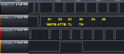
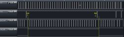
Take look that CHR-A10 is changing on both edges of PPU_!RD which might reveal how the MMC5 ppu cycle counter is implemented (if I'd do that in VHDL, everything would change on the falling edge)
5. The counter is not only counting passing edge of PPU_!RD but it also looks at the addresses. So if PPU will be fetching from $0000, $0001, $0002, $0003, etc - it will not work. There must be some more logic underneath that.
6. The counter won't count passing scanlines - if the frame has even 400 scanlines, the above logic will work for all of them.
krzysiobal wrote:
* at least one of those bits ($2000.3 or $2000.4) is written with 1
Typo? $2001?
—
What happens if a scanline has more than 170 reads?
Way back on page 5, I found a clue that there is at least 1 undiscovered writable register in range $512C-512F that behaves in some way similar to $512B. Not sure what I was doing now, but here it was:
viewtopic.php?p=227686#p227686Ben Boldt wrote:
Changing my random address range to be $5120 to $512B, it locked up almost immediately. Reducing the range to $5120 to $512A allowed the PPU bank to keep dancing all over indefinitely. So, writing to $512B can cause the lockup of the PPU bank. Maybe it is waiting for additional PPU reads, etc - I am not familiar with this.
Then, specifically excluding $512B from address range $5000 to $52FF, it still was able to lock up. I then excluded the range $512B to $512F, and now it does not lock up. Therefore, there is at least 1 more register in that range that behaves similar to $512B.
Quote:
Typo? $2001?
Sorry, of course you are right - $2001.
Quote:
What happens if a scanline has more than 170 reads?
Sprite banks are never asserted again in that scanline, so the counter does not wrap.
Quote:
Way back on page 5, I found a clue that there is at least 1 undiscovered writable register in range $512C-512F that behaves in some way similar to $512B. Not sure what I was doing now, but here it was: viewtopic.php?p=227686#p227686
When MMC5 is in `in-FRAME` mode, it uses:
->when in 8x8: $5120-$5127 for both sprites/backgrounds
->when in 8x16 $5120-$5127 for sprites & $5128-$512b for backgrounds (how is that detected - written above)
When MMC5 is in `outside-FRAME` mode, it uses:
->when in 8x8: $5120-$5127
->when in 8x16 $5120-$5127 or $5128-$512b (which one - depends on which to which one you last wrote).
If you write $2000.5=0 then automatically $5120-$5127 are activated and writing to $5128-$512b no longer makes effect.
On Power-UP, MMC5 uses 8x16 mode.
So if you mistakenly wrote to any of $5128-$512b, then MMC5 ignores the contents of $5120-$5127.
Buf If you write to any of $5120-$5127, it will again use those regs.
And I wrote to any of $512c-$512f and nothing was locked and even MMC5 still used $5120-$5127 which confirms there are NO regs in $512c-$512f range.
krzysiobal wrote:
And I wrote to any of $512c-$512f and nothing was locked and even MMC5 still used $5120-$5127 which confirms there are NO regs in $512c-$512f range.
My test was very uncontrolled, but I can say a few things that did and did not happen. I will try to rerun that test Monday evening and gather more details this time.
- PPU Address bits were not changing, I believe they were all 1s.
- PPU /RD never changed
- M2 toggled super slow, always would have been triggering reset
- When I set the test to write random data to $5120-512A, CHR-ROM Address bits would dance around endlessly.
- If I included $512B in this range, the address bits would no longer dance around (I called this "locked up").
- If I wrote random data to $5120-512F, excluding $512B, it would also lock up, therefore my conclusion that whatever locked it up with 512B, something else in $512C-512F had that lock up effect as well.
We can't dismiss my observation just yet krzysiobal! You had not gotten anything to lock up yet so I have more work to do to demonstrate how to lock it up. I don't know what it means so let's investigate!
I had actually lost that original test but I was able to get it to do it again after a lot of horsing around. It is very finicky and very difficult to nail down any sort of consistent behavior. Bear in mind, this whole exercise may be an artifact of my setup being marginal or invalid.
My setup has a starting point where I write a random byte to a random address in the range $5120-5127. My CHR Address bits all change randomly, no visible patterns. This is shown graphically in my GUI, so I am just watching the bits change and not finding a pattern. CHR A19 and A18 are always 0 in this test and A17-A10 are random.
When I expand the range to $5120-5128 into this test, now I can see partterns in the CHR bits. It will toggle between 2 values, then move on randomly, toggle between 2 new values, move on randomly, etc. Expanding to $5120-512B produces similar behavior. I am probably witnessing 8x16 sprite behavior with 2 values thing.
That was like that for a long time. Then suddenly it was A19 to A12 that were random and then A11 and A10 were coming from the PPU address bus. Not sure what I did to make that change but whatever it is got stuck doing it that way now.....
Earlier yet, when I added a read of $5208, it would keep updating the CHR address bus when writing randomly in the range $5120-512A and locked up when including $512B in the range, just like before, I was very excited, I definitely touched on what I was seeing before. I went back and forth at least 10 times doing various things (described in a moment) and it did it consistently. Not sure what I did but NOW, any time that I have the $5208 read in there it locks up no matter the range, even if I keep it to $5120-5127. And in fact, I change the read to some other address and it locks up, which points away from any connection to $5208 specifically. If I take away the read, it goes back to normal. I did in fact save a copy of the code that depended on $512B being in the mix and it too does not behave the same anymore. So apparently I have a moving target here. I inconsistently power cycle the MMC5 in this testing, but when I do, I remove power for a couple seconds... Maybe I broke something because it never does it now and I have been dorking around with it for a long time now, it is getting pretty late actually.
When it was locking up with $512B, I noticed that if I had it unlocked with range only to $512A, it would dance only between 2 values with the read in there. One of the values was CHR A19,18=0,0, A17-A10=all 1s, the other value it toggled to was a random value that stayed the same. If I changed my PPU address bus, it didn't change this value, but I noticed that when I went below $0C00, it was always CHR A19,18=0,0, A17-A10=all 1s, no longer toggling. Changing the PPU address back above $0C00, toggled again, still to that same value that got latched before. All the while writing random data to $5120-512A. I tried lots of PPU addresses. Very consistent cutoff at $0C00.
Once locked by writing to $512B, it could not be unlocked by simply stopping writing to $512B and keeping writing to $5120-512A. With $512B removed, if I removed the read, it would unlock, first toggling between the 2 old values for a moment then proceeding like normal. and I could add the read back and it would stay unlocked. Adding $512B back locked it again. I did this in several cycles. Things changed for some reason and none of this is repeatable anymore.
I think I am a little tired of chasing these things that keep changing on me. This is using my old slow setup without the microcontroller where reads and writes worked really well. My guess is that it is a setup issue somehow, I probably have the wrong edges of M2 or something but I just can't explain how the behavior keeps changing on me if my incorrect setup is staying incorrect.
Edit:
The RAM chips have been shipped! At least some good news today.
In hindsight, I think I moved to whitebox style testing with this particular thing too early. I got lots of different things to happen, which are all advancements to the understanding of a black box, but with the whitebox mentality I had, I rushed and pushed through those things trying specifically to find my preconceived pattern, which didn't really show up as expected. I think that was my main error tonight.
Ben Boldt wrote:
That was like that for a long time. Then suddenly it was A19 to A12 that were random and then A11 and A10 were coming from the PPU address bus. Not sure what I did to make that change but whatever it is got stuck doing it that way now.....
That
really really sounds like a spurious write to $5101
lidnariq wrote:
Ben Boldt wrote:
That was like that for a long time. Then suddenly it was A19 to A12 that were random and then A11 and A10 were coming from the PPU address bus. Not sure what I did to make that change but whatever it is got stuck doing it that way now.....
That
really really sounds like a spurious write to $5101
Yes, that makes perfect sense, a very good clue into my setup. I think you are really onto something with spurious writes because I do not currently have a solid understanding of how a write works. I had experimented at one point tonight expanding the range down to $5000, which could have done it once intentionally, but I also did power cycles and it persisted somehow or got written to spuriously again. There are too many variables in my setup right now I think.
One good thing is that the read in this situation is always locking it and it theoretically should not be doing that. I suspect my attempt to read screws up the sequence for the next write or something. It seems approachable to debug that.
When does a write get registered? Here is my understanding:
- The CPU can only read with M2 high. I base this on my observation that with M2 Low, MMC5 does not drive the data bus.
- To register a read, for example, to clear an interrupt flag, I believe that the CPU would drive the register's address with M2 low, set CPU R/W high, and the rising edge of M2 would count as the read that clears the interrupt flag.
- To register a write, I am not sure. Either:
A. With M2 low, the CPU would drive the register's address and data and then set CPU R/W low, and the rising edge of M2 would register the write (??)
B. With M2 low and CPU R/W high, the CPU would drive the register's address and data and the falling edge of CPU R/W would register the write (??)
C. With M2 high, the CPU would set CPU R/W low, then drive the register's address and data, and the falling edge of M2 would register the write (??)
I really do not know if it is A, B, or C, if you wouldn't mind letting me know, thanks
With the 6502/2A03, φ2/M2 high means "data bus is active", regardless of whether it's reading or writing.
As to exactly how the MMC5 is reacting to M2, I can only guess. It could be transparent latches or triggered by some edge of M2. It's even conceivable that different functions inside the MMC5 could work differently. But I'd hunch most of the functions are transparent latches.
Regardless, in your emulator: you should always leave M2 low, change everything, and only then raise and then lower M2.
lidnariq wrote:
Regardless, in your emulator: you should always leave M2 low, change everything, and only then raise and then lower M2.
Oh wow, okay, that is definitely not what I am doing, that explains a lot. I will give it a try.
Ben Boldt wrote:
lidnariq wrote:
Regardless, in your emulator: you should always leave M2 low, change everything, and only then raise and then lower M2.
Oh wow, okay, that is definitely not what I am doing, that explains a lot. I will give it a try.
I am having nothing abnormal or inconsistent now that I am writing and reading in that way, thanks a lot. I will also update my fast setup to work that way, hopefully that will fix it too.
I have a question for you guys. Is it possible to get the 2A03's DMC to do its fetches anywhere in the range $8000-BFFF but to also keep it silenced somehow? In this case, the MMC5 DAC's read mode and $00 delimiter interrupt might make more sense.
No.
While you can start the DPCM DMA at $FFC0, wait for it to overflow from $FFFF to $8000, and then fetch up to another $FB1 bytes from the bottom of the address space, its DAC can't be disabled.
lidnariq wrote:
No.
While you can start the DPCM DMA at $FFC0, wait for it to overflow from $FFFF to $8000, and then fetch up to another $FB1 bytes from the bottom of the address space, its DAC can't be disabled.
I wouldn't have thought so. Bummer... It is really hard to think of a reasonable way to use this DAC. Using the timer interrupt, trying to follow and update a 16-bit pointer, servicing other interrupts, it all seems like a deal breaker for any sort of reasonable sample rate without stopping everything else. The patent says it is "TWICE AS EFFICIENT" because you only have to read and not write. With our current understanding, the gain in efficiency is almost nothing compared to the overhead to get there via interrupt and keep track of and increment a 16-bit address.
The only timed DMA is that DMC, which is going to try playing the raw sample data and producing garbage sound off of it. The thought crossed my mind that the DMC would be 8x higher sample rate than the MMC5 DAC, and maybe a way to make the garbage ultrasonic, but it doesn't take more than a second to realize that won't work. White noise, frequency * 8 = white noise. The effort put into this by Nintendo, and patenting it, there ought to be a good way to use it.
I will spend some time trying to read the patent carefully tonight. I am sure that this has all been done and thought of before but I will give it a try anyway.
Edit:
I am really doing some reading between the lines in the patent here and letting my imagination run away, with extreme biases, which might be a bad thing. So bear with me.
In column 4, line 40, it says "On the other hand", suggesting that what follows is a separate aspect than what had been described previously. Definitely after this phrase, it begins describing DAC read mode and write mode as we already understand. But it seems that before this line, they could be describing some other aspect or mode of the DAC.
Focusing on column 4, lines 4-39 with predisposition that that this could describe a different function. In this section, they describe the audio data, and its layout, connected with Figure 2. This figure specifies that the audio data is stored in incrementing order, in the address range $8000-BFFF, and that each sound sample ends with $00.
Column 4 Line 28 wrote:
If a first address (that is, a start address) of a desired quantized data train is designated, quantized data are continuously and sequentially read until the stop code is detected.
"continuously and sequentially read" is very odd to me, if you were to do that in read mode as we understand it, it would play with extremely high sample rate. The way I read it, the word "continuously" means that there literally is no delay between reads. Maybe it is just worded funny but it seems strange and important.
Furthermore, proceeding with the next sentence, column 4, line 31:
Column 4 Line 31 wrote:
To this end, start address data for designating a start address of a certain quantized data train (X, Y, or the like) is stored in advance in a certain address in the program data storage area 14a.
This might have meant that your ROM program code keeps track of the start address of the sound data, but the next sentence:
Column 4 Line 35 wrote:
The address corresponds to a timing when a desired sound corresponding to the quantized data train is to be generated.
That sounds like you store/write a start address into a certain/particular address in program space, and it will start doing whatever it does (i.e. loading data all at once "continuously and sequentially") to play the sound that corresponds to that start address.
Also mentioned here and there is a "temporary storing means" on address/data bus 2, i.e. bus 2 meaning inside the cartridge and not inside the Nintendo. It is not clear if this is a RAM area or if it is just 1 byte storage, maybe only referring to item 16 in figure 3. Not sure.
Coming at this whole thing from a different angle, if we were Nintendo and wanted to make something that could play the DAC very efficiently, how would we do that?
Here is an idea of my own design, restricted to not violating anything described in the MMC5 DAC patent.
Let's say that memory range $8000-BFFF is all nice and full of $00-delimited PCM sound data. Let's also say that there is a magic "DAC playback rate" and "DAC start address" register somewhere. This would be a 1-byte address, corresponding to 64-byte chunks of range $8000-BFFF, i.e. actual address = (byte * 64) + $8000. And the playback rate would correspond to an M2 clock cycle count at which to update the DAC. Once the start address is written, an interrupt occurs. MMC5 disables ROM and replaces the interrupt vector with the actual address corresponding to the DAC start address, so the CPU literally goes there to fetch an instruction. During the level and/or edges of the clock where the CPU grabs the instruction, the MMC5 disables RAM and ROM, and drives a NOP (i.e. $EA) onto the data bus. On the other part of the clock, the MMC5 enables the RAM or ROM and stores the actual PCM data into its own "temporary storage means" / internal RAM. The CPU continues doing NOPs
continuously and sequentally, allowing the MMC5 to fetch all PCM data into its RAM extremely rapidly. When it encounters a $00, it simply changes its NOP instruction to an RTI instruction, and all is resumed, the MMC5 playing the PCM audio on its own time until it hits that $00 delimiter.
This is a made-up story, I am not asking anyone to believe this. Please think about it to make your mind go new places and let us know if any ideas happen.
Enough pretending, I am trying to figure out the most efficient way to use the DAC in read mode now. Here is the best I have come up with:
Set IRQ vector to address $010C.
RAM locations, initialized to:
$FC = Hardware timer reload value (setting to $00 stops the timer, non-zero sets the DAC sample rate)
$FD,FE,FF = LDA $8000 ; Cause DAC update by reading
$100,101 = INC $FE ; Increment the low byte of the LDA instruction at $FD.
$102,103 = BNE $02 ; Skip next instruction if previous increment did not roll over.
$104,105 = INC $FF ; Increment the high byte of the LDA instruction at $FD.
$106,107 = LDA $FC
$108,109,10A = STA $5209 ; Restart or stop Hardware Timer based on $FC value
$10B = RTI ; Exit immediately. Other pending interrupts will presumably cause reentry and be handled per $111.
IRQ Entry:
$10C,10D,10E = LDA $5209
$10F,110 = BNE $EC ; i.e. goto $FD if hardware timer interrupt flag is set.
$111,112,113 = JMP $xxxx ';i.e. Go to normal IRQ handler
Normal IRQ handler will check for DAC IRQ and be handled by setting $FC = 0.
When you want a DAC sound to play, set DAC to read mode, set address $FE,FF to the starting address of the sound data, and set $FC as the period corresponding to the sample rate of your DAC data, and then write $01 to $5209 to trigger the first hardware timer interrupt.
I calculate that the above method would take the following number of cycles to run (please correct me if there are errors):
LDA $8000 -> 4
INC $FE -> 5 (zero-page inc)
BNE $02 -> 2
INC $FF -> 5/256 (zero-page inc, only 1 out of 256 times)
LDA $FC -> 3
STA $5209 -> 4
RTI -> 6
IRQ Entry: -> 7
LDA $5209 -> 4
BNE $EC -> 2
Total = 37.02 cycles.
The NES CPU is 1,790,000 cycles/second
100% CPU usage would be 1,790,000/37.02 = 48352 DAC samples / second.
Now backwards to find %CPU usage at 11.025 kHz DAC sample rate:
1,790,000/11,025 = 162.36 CPU cycles occur each DAC update
37.02 / 162.36 = 22.8%! And therefore 22.050kHz audio = only 45.6% CPU
It seems 8-bit, 11 or 22 kHz uncompressed audio is reasonably possible??
Note that you're trashing A there (only P is saved by the hardware), so that's not usable with anything in the main thread.
As far as I can tell, the "set DAC on contents of read from $8000-$BFFF" is only useful for skipping an extra stX $5011; nothing better.
lidnariq wrote:
Note that you're trashing A there (only P is saved by the hardware), so that's not usable with anything in the main thread.
Embarrassed to say so but I did not know that. That is nice though, I guess -- it lets you pick and choose what you want to push and pull. I see that S and P are saved by hardware when an interrupt occurs and just P when you do a JSR, thus the difference between RTS and RTI. Is there a good throw-away read method, or am I going to have to add a push and a pull?
lidnariq wrote:
As far as I can tell, the "set DAC on contents of read from $8000-$BFFF" is only useful for skipping an extra stX $5011; nothing better.
It does seem per the patent at face value that the STX would be the only savings. But on a resource constrained system like this, I think it makes an actual difference. A 4-cycle savings at 22 kHz represents 22,050 * 4 = 88,200 cycles per second saved. 88,200/1,790,000 = 4.93% CPU capacity recovered. It is definitely not a 50% savings, or any savings of program space or "a programmer's time to write the code" as they seem to suggest in the patent. That troubles me big-time. Probably written by some self-righteous hardware guy that thought he made the world better.

And did.
There is the definite possibility that this feature really isn't as great as they say, and there is nothing more to it than what we already understand. We have to drive past that and keep thinking in different ways if we are going to have a chance to find something. We can only find things if we look at new angles and/or in new places, telling stories, Ouija boards, whatever it takes.
I think that this code, if fixed and modified, makes it possible to use the DAC, and I think that's a step in the right direction.
Another question for you -- How does the IRQ interact with V-blank? As I understand, V-blank and IRQ are 2 separate interrupts, each with their own vector. Can an IRQ interrupt happen from within a V-blank interrupt?
Edit:
How about this:
$FC = Hardware timer reload value (setting to $00 stops the timer, non-zero sets the DAC sample rate)
$FD,FE,FF = INC $8000 ; Cause DAC update by reading, non-destructive read
$100,101 = INC $FE ; Increment the low byte of the LDA instruction at $FD.
$102,103 = BNE $02 ; Skip next instruction if previous increment did not roll over.
$104,105 = INC $FF ; Increment the high byte of the LDA instruction at $FD.
$106,107 = LDA $FC
$108,109,10A = STA $5209 ; Restart or stop Hardware Timer based on $FC value
$10B = RTI ; Exit immediately. Other pending interrupts will presumably cause reentry and be handled per $111.
IRQ Entry:
$10C,10D,10E = LDA $5209
$10F,110 = BNE $EC ; i.e. goto $FD if hardware timer interrupt flag is set.
$111,112,113 = JMP $xxxx ';i.e. Go to normal IRQ handler
INC $8000 ->
6 (+2 from before)
INC $FE -> 5 (zero-page inc)
BNE $02 -> 2
INC $FF -> 5/256 (zero-page inc, only 1 out of 256 times)
LDA $FC -> 3
STA $5209 -> 4
RTI -> 6
IRQ Entry: -> 7
LDA $5209 -> 4
BNE $EC -> 2
Total = 39.02 cycles.
11.025 kHz:
39.02 / 162.36 = 24.03%
22.050kHz:
*2 = 48.07% CPU
Edit 2:
Ooops I still used A. That won't work.
Ben Boldt wrote:
Another question for you -- How does the IRQ interact with V-blank? As I understand, V-blank and IRQ are 2 separate interrupts, each with their own vector. Can an IRQ interrupt happen from within a V-blank interrupt?
A normal IRQ can happen within V-blank as long as the interrupt disable flag in the processor status register is cleared (it's set to 1 automatically when the interrupt handler is entered, but you can clear it in code with CLI to allow overlapping interrupts). V-blank uses the NMI (non-maskable interrupt) so it will trigger regardless of the state of the interrupt disable flag.
Ben Boldt wrote:
Is there a good throw-away read method, or am I going to have to add a push and a pull?
Because self-modifying code, sure?
Say you have
Code:
a: BIT $8000
INC a+1
BNZ done
INC a+2
done:
Quote:
How does the IRQ interact with V-blank?
NMI is reentrant. Any time /NMI line falls, the CPU will load the NMI vector, push the return address onto the stack, push the flags, and disable interrupts.
IRQ isn't. If interrupts are enabled, when the /IRQ line is low, the CPU will load the IRQ vector, push the return address onto the stack, push the flags, and
still disable interrupts. As thefox points out, either interrupt handler can cooperate and re-enable interrupts. Won't help in case of OAM DMA, though.
Quote:
$106,107 = LDA $FC
$108,109,10A = STA $5209 ; Restart or stop Hardware Timer based on $FC value
Still trashing A here. I think the only way you could detect completion without using A/X/Y is by detecting underflow from $8000 to $7FFF:
Code:
a: BIT $8000
INC a+1
BNZ cont
DEC a+2
BMI cont
RTI
cont: DEC $5209
LSR $5209
RTI
... and restarting the cycle-timed IRQ is even worse.
Ugly. At 12cy here, and 14cy for
PHA / LDA zp / STA $5209 / PLA, it's not worth it unless you specifically want 6.4kHz (just DEC) or 12kHz (DEC and LSR).
You'd also have to structure the PCM as blocks of 256 played forward, blocks backwards. Assuming 6.4kHz and the BIT instruction's operand is in zero page, typical overhead: 18+14cy, worst case 26+14cy. (14cy being unavoidable IRQ+RTI overhead)
Might it have been meant for a looping 256-entry wavetable in ROM, where the main program uses the IRQ's rate to control the playback frequency?
Noted on the re-entrant IRQ stuff, good to know. I see where OAM DMA could be a problem. Does that take a long time? If so, I suppose that would need to be turned off for the duration of the sound to prevent audible glitches? That seems potentially crippling.
lidnariq wrote:
Quote:
$106,107 = LDA $FC
$108,109,10A = STA $5209 ; Restart or stop Hardware Timer based on $FC value
Still trashing A here.
Yeah I noticed... My bad.
tepples wrote:
Might it have been meant for a looping 256-entry wavetable in ROM, where the main program uses the IRQ's rate to control the playback frequency?
Sounds cool, like a Namco-163 channel without amplitude/envelope control? So a lot like the triangle channel but with custom wave shape? That would definitely be a new type of sound. I have not looked into FDS audio for potential similarities. The patent also mentions this interesting note in column 4 line 20:
MMC5 DAC Patent wrote:
The quantized data is not limited to one obtained by quantizing music played by a musical instrument or a human voice and subjecting the same to pulse code modulation (PCM). For example, the quantized data may be one prepared with a programming method by an input device such as a keyboard.
This seems to suggest that either the game itself could be written to change its DAC based on inputs (such as the controller or famicom keyboard) or a wave shape could be programmed into the game, wavetable style.
lidnariq wrote:
I think the only way you could detect completion without using A/X/Y is by detecting underflow from $8000 to $7FFF:
Code:
a: BIT $8000
INC a+1
BNZ cont
DEC a+2
BMI cont
RTI
cont: DEC $5209
LSR $5209
RTI
... and restarting the cycle-timed IRQ is even worse.
Ugly. At 12cy here, and 14cy for
PHA / LDA zp / STA $5209 / PLA, it's not worth it unless you specifically want 6.4kHz (just DEC) or 12kHz (DEC and LSR).
You'd also have to structure the PCM as blocks of 256 played forward, blocks backwards. Assuming 6.4kHz and the BIT instruction's operand is in zero page, typical overhead: 18+14cy, worst case 26+14cy. (14cy being unavoidable IRQ+RTI overhead)
Very clever using the DEC $5209, that took me a few minutes to understand that one. In theory, with your same code intact, you could use the DAC interrupt to change a+1 and a+2 to trick it to end arbitrarily when the data has a $00 in it, so you don't always have to end necessarily at $7FFF.
Edit:
Considering PHA/PLA, it looks like you could save 1 cycle by doing STA/LDA into zeropage RAM instead of using the stack.
Ben Boldt wrote:
In theory, with your same code intact, you could use the DAC interrupt to change a+1 and a+2 to trick it to end arbitrarily when the data has a $00 in it, so you don't always have to end necessarily at $7FFF.
I mean, sure, you could poll $5010 at the end of the handler here. More time in the interrupt means less time
Quote:
Considering PHA/PLA, it looks like you could save 1 cycle by doing STA/LDA into zeropage RAM instead of using the stack.
Yeah, I forgot midway that I was assuming self-modifying code.
—
Tepples's comment about a wavetable synth suggests to me that maybe the ultra-lightweight version of the IRQ code could be used just like the FIFOs in the GBA / Quietust's DRIPGAME
Ultimately, though, the problem is that you can't do
anything else in the memory region from $8000-$BFFF, so those banks are almost completely useless to the programmer. You have to run your entire program out of $C000-$FFFF and whatever you copy into RAM in $6000-$7FFF.
lidnariq wrote:
Ben Boldt wrote:
In theory, with your same code intact, you could use the DAC interrupt to change a+1 and a+2 to trick it to end arbitrarily when the data has a $00 in it, so you don't always have to end necessarily at $7FFF.
I mean, sure, you could poll $5010 at the end of the handler here. More time in the interrupt means less time
Yes, but this would be in the regular IRQ handler and not the DAC update IRQ, so it would be checking it only as often as any other IRQs occur which is much less frequent.
lidnariq wrote:
Quote:
Considering PHA/PLA, it looks like you could save 1 cycle by doing STA/LDA into zeropage RAM instead of using the stack.
Yeah, I forgot midway that I was assuming self-modifying code.
—
Tepples's comment about a wavetable synth suggests to me that maybe the ultra-lightweight version of the IRQ code could be used just like the FIFOs in the GBA / Quietust's DRIPGAME
Ultimately, though, the problem is that you can't do
anything else in the memory region from $8000-$BFFF, so those banks are almost completely useless to the programmer. You have to run your entire program out of $C000-$FFFF and whatever you copy into RAM in $6000-$7FFF.
Yes that is a pretty big problem that the DAC read mode hogs up so much address space. I hadn't thought of that. Changing in and out of read mode within the interrupt doesn't make sense, it is more expensive than actually doing the write manually to the DAC. In fact, if it comes to that, it isn't really much benefit at all versus manual writes to the built-in DAC, nothing really helped anything... It seems that the patent is written emphasizing how this feature makes things more efficient. It doesn't really even mention any gain in sound quality. We must be missing something still. Maybe some testing of DAC read mode range vs. PRG mode is in order.
I am still poking at this source code, I think it could lead us to unexpected places by working through it.
Updated code with suggestions:
Code:
a: (@$FD)
BIT $8000
INC a+1
BNE b
INC a+2
b ROR (skip for 11.26kHz, keep for 18.45kHz)
STX $5209
LDX $FC ; pull X
RTI
IRQ_ENTRY:
STX $FC ; push X
LDX $5209 ; X is known to be $80 if hardware timer caused interrupt.
BNE a
JMP NORMAL_IRQ
NORMAL_IRQ:
; Check for DAC IRQ
; Normal IRQ stuff
LDX $FC ; pull X
RTI
Calculations:
Code:
Number of cycles between timer IRQ and restarting timer without ROR:
a: (@$FD)
BIT $8000 4
INC a+1 5
BNE b 2
INC a+2 5/256
b STX $5209 4 ; Timer starts
LDX $FC 3
RTI 6
IRQ_ENTRY: 7
STX $FC 3
LDX $5209 4
BNE a 2
Total until timer restart = 7+3+4+2+4+5+2+(5/256)+4 = 31.0195 cycles.
Number of cycles per timer IRQ, considering loading with $80(=128) + 31.0195 = 159.0195
1.79MHz / 159.0195 = 11.2565kHz
CPU usage calculation:
Total CPU cycles per second = 1,790,000
Total DAC updates per second = 11,256.5
Total CPU cycles to update DAC = 31.0195+3+6 = 40.0195
Total CPU cycles to update DAC per second = 11,256.5 * 40.0195 = 450,479.5
% CPU Usage = 450,479.5 / 1,790,000 = 25.17%
Code:
Number of cycles between timer IRQ and restarting timer [u]with[/u] ROR:
a: (@$FD)
BIT $8000 4
INC a+1 5
BNE b 2
INC a+2 5/256
b ROR 2
STX $5209 4 ; Timer starts
LDX $FC 3
RTI 6
IRQ_ENTRY: 7
STX $FC 3
LDX $5209 4
BNE a 2
Total until timer restart = 7+3+4+2+4+5+2+(5/256)+2+4 = 33.0195 cycles.
Number of cycles per timer IRQ, considering loading with $40(=64) + 33.0195 = 97.0195
1.79MHz / 97.0195 = 18.4500kHz
CPU usage calculation:
Total CPU cycles per second = 1,790,000
Total DAC updates per second = 18,450
Total CPU cycles to update DAC = 33.0195+3+6 = 42.0195
Total CPU cycles to update DAC per second = 18,450 * 42.0195 = 775,259.8
% CPU Usage = 775,259.8 / 1,790,000 = 43.31%
Edit:
Using DAC Write Mode, not terribly worse than what we had and doesn't hog address space:
Code:
Number of cycles between timer IRQ and restarting timer [u]with[/u] ROR (faster sample rate):
a: (@$FD)
ROR 2
STX $5209 4 ; Timer restarts here
LDX $8000 4
STX $5011 4
INC a+1 5
BNE b 2
INC a+2 5/256
b LDX $FC 3
RTI 6
IRQ_ENTRY: 7
STX $FC 3
LDX $5209 4
BNE a 2
Total until timer restart = 7+3+4+2 + 2+4 = 22 cycles.
Number of cycles per timer IRQ, considering loading with $40(=64) + 22 = 86
1.79MHz / 86 = 20.8140kHz
CPU usage calculation:
Total CPU cycles per second = 1,790,000
Total DAC updates per second = 20,814
Total CPU cycles to update DAC = 22 + 4+4+5+2+(5/256)+3+6 = 46.0195
Total CPU cycles to update DAC per second = 20,814 * 46.0195 = 957,849.9
% CPU Usage = 957,849.9 / 1,790,000 = 53.51%
Careful:
ROR in isolation modifies A, and you haven't saved A here.
Also, I misunderstood earlier what reads from $5209 contained (I'd misunderstood it to be the current timer value. It isn't...) So INC, DEC, and LSR are the useful instructions to use here because the register should reliably hold $80 if the interrupt is called(right??). Yielding periods of 7+6+(127,129,64) → rates of 12784, 12969, 23244 Hz ... those aren't too shabby.
The bit I had with the label "a" was specifically about modifying the operand to the instruction that reads the data for the DAC.
Managing multiple different sources of IRQs is kind of a pain on the NES, because IRQ flags clear themselves when read. It makes me personally inclined to say that it's not worth it.
If we assume a mixing FIFO, the fastest anything we could manage would be
Code:
IRQ:
INC $5209 ; 6cy, converts 0x80 (IRQ enabled) to 0x81 (period 129+6+7)
addressinginstruction: BIT $8000
INC addressinginstruction+1
RTI
but the main mixing code would need to refill it at 103Hz, which is too fast to be useful in a normal 60Hz world.
lidnariq wrote:
Careful: ROR in isolation modifies A, and you haven't saved A here.
Oh crap, nice catch. I shouldn't have switched over to using X I guess.
lidnariq wrote:
Also, I misunderstood earlier what reads from $5209 contained (I'd misunderstood it to be the current timer value. It isn't...) So INC, DEC, and LSR are the useful instructions to use here because the register should reliably hold $80 if the interrupt is called(right??). Yielding periods of 7+6+(127,129,64) → rates of 12784, 12969, 23244 Hz ... those aren't too shabby.
I am a little stuck how to use INC/DEC/LSR on the timer IRQ flag. By doing those instructions, you acknowledge the IRQ and restart the timer with your shifted/dec'd value all in one go, that is super awesome. But I think you have to check the flag first so you can skip the whole timer restart and DAC update if it wasn't set.
lidnariq wrote:
The bit I had with the label "a" was specifically about modifying the operand to the instruction that reads the data for the DAC.
Managing multiple different sources of IRQs is kind of a pain on the NES, because IRQ flags clear themselves when read. It makes me personally inclined to say that it's not worth it.
I can agree with that mentality. For example, I would not entertain the idea of self-writing code like this where I work. I would have the company get a nicer micro and avoid the risk of such a crazy approach. But with this, we get what we get and there might be necessary evils... At least in this case, we might be able to hash out a robust method of handling multiple IRQs and then just sort of forget about it and let it do its thing. Until it comes back to bite us of course! I do get what you are saying.
lidnariq wrote:
If we assume a mixing FIFO, the fastest anything we could manage would be
Code:
IRQ:
INC $5209 ; 6cy, converts 0x80 (IRQ enabled) to 0x81 (period 129+6+7)
addressinginstruction: BIT $8000
INC addressinginstruction+1
RTI
but the main mixing code would need to refill it at 103Hz, which is too fast to be useful in a normal 60Hz world.
Per my previous comment, I think that works if the timer is the only IRQ, or if spurious extra DAC updates are acceptable when other IRQs occur. In this case, you would get 1 extra DAC update before it was due, and then you would restart the timer with value $01, which causes 1 additional DAC update almost right away again. I am not sure what this would sound like -- it might be acceptable. We would have to try it and see what it sound like.
Ben Boldt wrote:
I am a little stuck how to use INC/DEC/LSR on the timer IRQ flag. By doing those instructions, you acknowledge the IRQ and restart the timer with your shifted/dec'd value all in one go, that is super awesome. But I think you have to check the flag first so you can skip the whole timer restart and DAC update if it wasn't set.
lidnariq wrote:
It makes me personally inclined to say that it's not worth [having an interrupt handler that handles multiple IRQ sources at the same time].
I mean, that's all there is to it. You build a robust heavy-weight system that can handle a bunch of different interrupt sources (although, in practice, a "bunch" may be "two" because only MMC5's cycle and scanline IRQs seem to be useful here), or you build something lightweight and don't let yourself use all the features simultaneously.
So if by definition, the only IRQ you're using is the cycle IRQ, you don't need to check on it ... and you also know that a useful value will be there for a RMW instruction.
You may also be able to decide to start off by checking $5204 and leave the desired value in $5209 ... if those specific values were useful.
Quote:
I am not sure what this would sound like -- it might be acceptable. We would have to try it and see what it sound like.
Well, while OAM DMA is going, you lose 513 or 514 cycles regardless, during which the IRQ just doesn't get handled. The only real choice is to accept the audio glitches, or not use sprites.
lidnariq wrote:
Well, while OAM DMA is going, you lose 513 or 514 cycles regardless, during which the IRQ just doesn't get handled. The only real choice is to accept the audio glitches, or not use sprites.
I would say that a 513/514 cycle delay would not be acceptable unfortunately unless you use it to play an explosion sound effect or something that would naturally contain glitches like that. I don't like to admit it but this DAC does seem pretty hopeless.
A previous thread asking about streaming sound via the 2A03's DAC led me to generate
this simulation. Memblers had previously made hardware that did exactly this (streaming sound to the 2A03's DAC using interrupts) and shared some recordings from that system as well.
It's clearly bad, but I'm not convinced it's incontrovertibly bad.
So, with what we know about MMC5 versus using the 2A03 DAC, these are the advantages of MMC5:
- 8-bit DAC instead of 7-bit - slight quality improvement
- Linear DAC - slight quality improvement
- DMC can still run at the same time - could be useful, not sure
- DAC read mode, which has very slight benefits and major drawbacks
- Invokes unrealistic pipe dreams
And the MMC5 hardware timer IRQ would have equal benefits to either DAC, so that doesn't really count.
I think someone wanted a patent on their resume and didn't really give a crap whether it was useful or not, especially supported by the bogus statements in column 9 lines 3-18. That is my latest theory and it is frustrating.
I don't think the MMC5's features are about the patent—you'll notice that the JP filing date is months after we know they'd started manufacturing. Something staking out an IP claim for its own sake does that in the other order.
To me, it feels like trying to make lemonade out of a lemon.
I do find myself wondering why they didn't provide the ability to use the MMC5-internal RAM as a FIFO for the DAC, though.
I was thinking of a way to search for more writable registers. I had tried before to measure the current drawn by the MMC5 with my scope while writing to different registers. I did see lots of modifications to the current, especially at transitions, but thinking about it more, I had several errors in the way I connected it. I was using a low-side current sense resistor, meaning I put a resistor in series with GND and read the voltage across it. I had left my ceramics in place on the MMC5 breakout board, so I would not have seen the full spikes at each transition. I am thinking, I need a high-side current sense, all capacitors on the power supply side of the current sense. I can put my scope into AC mode to read from GND to outside the current sense resistor to see how big the current spike is at each transition. I can't read the DC current with a high-side current sense though unless I do something with an op-amp or a low-voltage diff-probe. I was thinking I would try it again with a better setup and check to see if I can find any patterns comparing known registers vs. non-existing registers. Also, alternating between $00 and $FF writes vs. writing the same value repeatedly, if that could be seen in the current. I am sure that there is stuff running and gates and multiplexers, etc, changing no matter where you write. But maybe it draws slightly more current as signals go more places if it is a valid register -- that is a theory that may or may not be true or measurable with my equipment.
I did not have luck last time but I think I should try again with a better setup.
I think it is time to move on from the DAC for a while. Looking at the big picture of the patent, it really focuses on read mode -- that is what they are patenting. They show it in comparison to write mode. I think that it is possible that there could be other ways of using the DAC that didn't pertain to explaining read mode. I don't think all hope is lost, but I also think it is time to move on to different things in the MMC5.
I got my setup running tonight that can look at the change in current drawn by the MMC5. I connected the MMC5 VCC only to a 10-ohm resistor, then on the other side of that resistor, tantalum and ceramic to GND, very close by. I then probed my scope from MMC5 VCC to GND and put it into AC coupled mode. It looks marvelous. I believe that this would be doing a repeated read of address $0000 in the scope shot, that is what my fast dsPIC-based setup does when it is idle now. Will work on expanding this to repeated writes of known registers tonight, in search of level shifts and how steep those oscillations go, hopefully correlating to something that can give us more clues. A good chance this will lead nowhere but you never know!
Attachment:
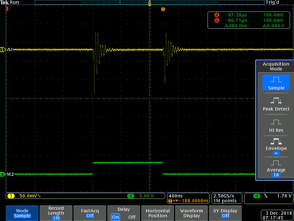 tek00037.png [ 26.94 KiB | Viewed 5104 times ]
Edit:
I am sorry to report, but I did not find anything correlating VCC current to valid addresses after spending all night trying different things. The most obvious test was to set a valid address (I chose $5000), CPU R/W = 0, data bus = $00, and toggle M2. Basically write $00 to $5000 repeatedly. Then compare this to address $6000 (invalid). I could find no differences at all in levels or oscillation shapes. Though my scope channel monitoring the current is in AC coupled mode, for the purpose of centering the waveform and letting me vertically zoom way in on it, the AC coupled time coefficient is WAY slower than this horizontal zoom level so I am actually able to measure relative current levels at different states of the test. They were the same as well.
I tried another test setting everything stationary and then just toggling CPU R/W. $5000 vs. $6000. Tried that test with M2 always high and M2 always low. Nothing found.
I tried the first test again, but between each M2 toggle, change invert the data bus, $FF/$00. These tests all made differences, but had identical results comparing $5000 to $6000.
I tried alternating between writing to $5000 and $6000 and other registers. This created varied results because I am toggling different numbers of address bits, so that test did not produce usable results. I guess I am sort of out of ideas now with this experiment, there aren't that many sequences to do these things in and all disturbances to the VCC current have looked absolutely the same to me whether the address is valid or not.
Ideas:
- I only read the current of VCC. I am not sure if there would be another place to probe current, such as CPU R/W. That seems a little doubtful to me.
- The way I probed is as tight as could be and works great. I am using 500MHz bandwidth on the scope. I do not believe that could be improved.
- Maybe toggling M2 way faster than normal (i.e. 100 MHz) to stack up switching losses within the MMC5, making normal operations take more current? Sounds like that could break it or give unreliable results
- Decap the MMC5
Do you guys have any insight or ideas that can coax this thing to reveal itself? Think analog and abnormal modes of operation. Anything I might have done wrong? Could my digital inputs be feeding the VCC, and I am not actually getting all of my current through the resistor where I am looking at it? Looking for brainstorming right now, there are no bad ideas, everything is accepted.
Edit 2:
More poking at it today, I tried setting MMC5 VCC to 5.4V, my logic's VCC to 4.6V to make sure none of my logic ended up higher than the MMC5 VCC to possibly feed it. I turned bandwidth limitation on and off. I tried using my scope's 512 sample average. Since my test is very stable, the average works great to dial in a little more precision, but still no patterns found.
All in all, I have discovered from these tests that my little level shifting FET circuit for each address pin is slow to rise because it does not have a strong enough pull-up resistor. That is useful and will improve my high-speed setup. Progress was made after all.
AND just as I wrote that, sitting here on the couch at home, I remember that these little FET circuits invert, and so all of these tests have been using the wrong addresses. I was taking the 16-bit address, inverting just A15 for /ROMSEL. I should have inverted A0-A14 and NOT inverted A15 for /ROMSEL. Will try again tomorrow. Will create a C macro so as not to make this mistake again.
Edit 3:
#define MACRO_CPU_ADDRESS(X) ((X) ^ 0x7FFF)
Bunch of random thoughts:
#1 I think the MMC5 is NMOS, so you've got a significant DC bias to extract a signal from
#2 You're talking about measuring the difference in charging current of a small handful of transistors, probably total capacitance on the order of fF. ( For example, the power consumption of a PIC16F84 can be pretty accurately modeled as an 83pF capacitor being charged and discharged repeatedly) Measuring this is going to require a lot more than a 10 ohm resistor.
#3 I'd be worried about losing signal in that 32MHz oscillation your 'scope trace. Ringing makes it hard to see anything else going on, and there's no intrinsic reason the ringing has to be there.
lidnariq wrote:
#1 I think the MMC5 is NMOS, so you've got a significant DC bias to extract a signal from
Would you explain this more? The signal I am looking at has 5V of DC bias, but I don't think I understand what you mean by NMOS bias.
Code:
n/c: AVcc X -----------------------------+-- +4.6V
10 Ohm _____|______ | ___________ ___|__
+5.4V --+---/\/\/--O-----| | v | |-----------|Lin |
| ^ | |-------| | 3.3V |Reg.|
tant --- Scope | MMC5 |-------| dsPIC | |____|
2.2u --- AC-couple | |-------| | |
+0.1u | v | |-------| | |
GND --+----------O---+-|__________| |_________|-+------------+-- GND
|________________________________|
lidnariq wrote:
#2 You're talking about measuring the difference in charging current of a small handful of transistors, probably total capacitance on the order of fF. ( For example, the power consumption of a PIC16F84 can be pretty accurately modeled as an 83pF capacitor being charged and discharged repeatedly) Measuring this is going to require a lot more than a 10 ohm resistor.
I can definitely experiment changing the resistor to a larger value. I didn't want 5V to dip too far so I chose a small value. The DC current drawn by the MMC5 changes measurably when I change CPU R/W with data bus floating.
lidnariq wrote:
#3 I'd be worried about losing signal in that 32MHz oscillation your 'scope trace. Ringing makes it hard to see anything else going on, and there's no intrinsic reason the ringing has to be there.
Do you think I should add cap across where the scope is connected? I thought I might lose fine details that might occur if I had any cap where I am measuring, that is why I have the ringing there intentionally. I removed a 0.1u ceramic surface mount cap I had put on the bottom side of the breakout board for this very reason. In my testing, I was actually measuring the peak of the ring at full bandwidth for any slight differences. It jumps around very slightly, amazing how stable and repeatable it is. I measured with re-triggering or with averaging to get a statistically good sample size to zero-in exactly on a particular level, which in my tests with all invalid addresses, proved very consistent.
I could try adding some cap and increasing my resistor. If the signal is on the order of charging fF (which I do not doubt is the case), adding even 1pF (i.e. my probe itself) would probably destroy it. But what the heck, I will try anyway. The very best we can hope for is clues from this type of test, and that is exactly what I will keep looking for with your suggestions.
Ben Boldt wrote:
Would you explain this more? The signal I am looking at has 5V of DC bias, but I don't think I understand what you mean by NMOS bias.
NMOS draws static power, so there's a constant voltage drop across your current sense resistor. Theoretically this is canceled out by your scope being AC coupled, I guess.
Quote:
I can definitely experiment changing the resistor to a larger value. I didn't want 5V to dip too far so I chose a small value. The DC current drawn by the MMC5 changes measurably when I change CPU R/W with data bus floating.
I'd be inclined to try an inductor. Changes in the current through it theoretically should show up larger that just the voltage change across a current sense resistor. ... of course, it could also break everything.
Quote:
Do you think I should add cap across where the scope is connected?
I think you want to know what's causing it. The power supply should be as firm as possible before you go into the current sense resistor so that you can get a useful measurement. This is really about managing signal-to-noise ratios. Oscilloscopes often only have an 8 bit ADC, so at the analog stage you need to get unwanted signals down to ... well, at least not a lot louder than your wanted signal.
Quote:
I thought I might lose fine details that might occur if I had any cap where I am measuring, that is why I have the ringing there intentionally.
While it's likely that the bypass cap would conceal the fine details ... it's also likely that the ringing is an order of magnitude or more larger than your actual signal. (10Ω, 100mV scale -> 10mA scale? almost guaranteed right now)
By the way, what's static and dynamic MMC5 current consumption? i.e. everything fixed, M2 low, PPU/RD+/WR high ... vs M2 oscillating ... vs PPU A13&/RD oscillating?
Early findings but I found very clear correlations with a few registers that do and do not exist:
Attachment:
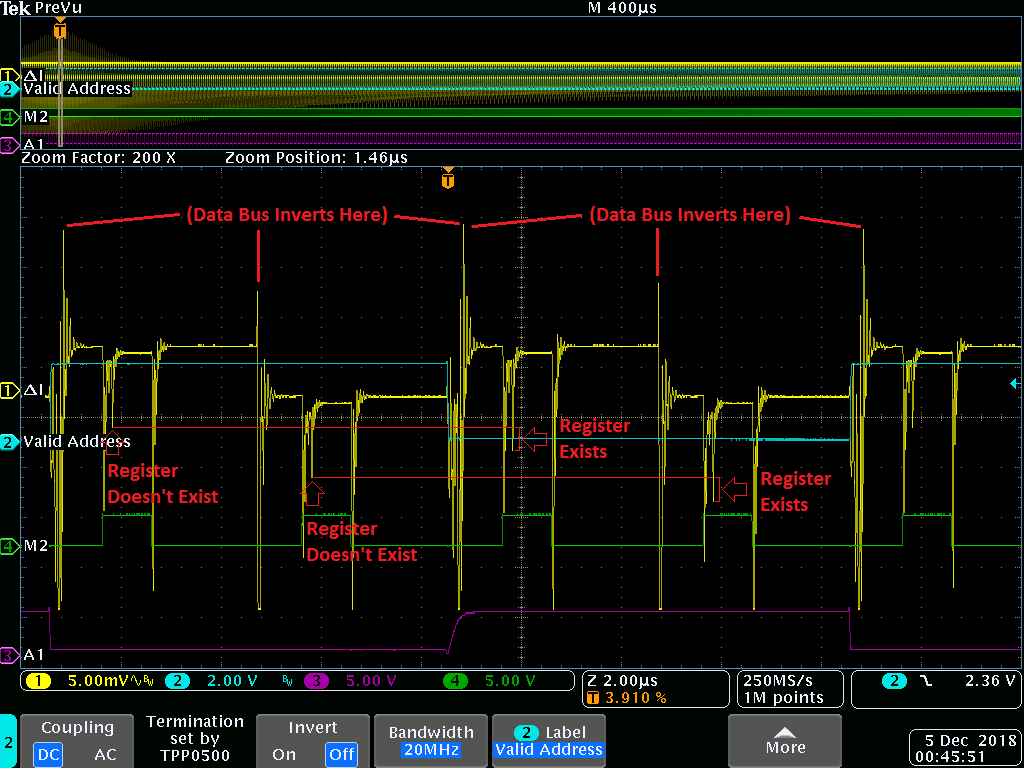 Register Existence.png [ 67.77 KiB | Viewed 5159 times ]
In this scope shot, a lower delta-I means a higher current draw by the MMC5. About 200 nsec after the rising edge of M2, something else has a small current spike. This current spike is large with registers $5000 and $5002 and small with registers $5020 and $5001. Comparing $5020 directly to $5001, they are the same. The scope shot compares $5020 ("valid address" signal high: invalid) to $5002 (valid address signal low: valid). Valid address is just an extra pin I am setting on the dsPIC. Also seen in the screenshot is CPU A1, demonstrating acceptable pull-up on address bus now that I changed that to 1k pull-ups today. The screenshot is a 512 sample average. I am triggering on my valid address signal. To verify that this difference is not an artifact of averaging or triggering somehow, I inverted the valid address signal, and spike still followed the valid address, i.e. the spike was present when valid address was high in that case.
This looks promising so far, will continue experimenting this evening.
Update:This
IS a highly effective way to see what registers are writable! I have found these registers to be writable:
5000
NOT 5001 (Confirms what we suspected, no pulse sweep unit)
5002
5003
5004
NOT 5005 (Confirms what we suspected, no pulse sweep unit)
5006
5007
5010
5011
5015
Unfortunately, nothing else until $5100
5100
5101
5102
5103
5104
5105
5106
5107
NOT 5110-5112 (Confirms what we suspected)
5113
5114
5115
5116
5117
5120
5121
5122
5123
5124
5125
5126
5127
5128
5129
512A
512B
NOT 512C-512F (Formally ending any remaining suspicion from my buggy tests from before)
5130
5200
5201
5202
5203
5204
5205
5206
5207 (Confirming this unknown register very likely exists)
5208
5209
520A
To do this, I set my scope in 8-sample average mode, running. I ran the same test with the invalid address and the valid address, but I added an I2C command that could change the valid address. In the GUI on my computer, I added a text box and button that would send a new address. The address auto-incremented after clicking the button. So I was able to keep clicking the button and watching the scope to test series of addresses efficiently. I found it best to set 1 horizontal cursor to the bottom of that magic dip on an invalid address and the other cursor to the flat spot right before it. Because the whole waveform shifts up and down slightly depending on the address, I would visually compare the distance between the cursors to the waveform. Anything larger than the cursors is writable. Addresses with only 1 or 2 writable bits had smaller but still detectable dips.
I tested all addresses in the range $5000 - 5250. I also tested these ranges and found nothing:
$5300-5310
$5400-5410
I tested $5800-5812 and they all DID have activity, similar to register $5204 with only 1 bit, for example. I then tested $5A00, it also behaved this way. I then tested $5C00, and it TOO behaved this way. This seems to suggest that RAM could exist in the entire range $5800-5FFF.
Next, I will experiment with the data written. Right now, I am alternating between writing $FF and $00. I will see if I can toggle just 1 bit at a time and see if I can tell which specific bits are writable.
Edit:
I am not able to tell any difference for individual bits. It seems that the current spike does not depend on the data written, only the number of writable bits. I will measure the deflections for each known register to get a rough idea how many bits are writable, but it won't tell us "which" bits. Also, some registers have a great big disturbance when written, presumably I trigger a bankswitch that changes lots of outputs or something. I recorded great big disturbances from writing to these registers:
5101
5105
5116
512B
5205
5206
I may be able to just always write the same value though instead of alternating $00 to $FF, and it may prevent this from happening. Will try it.
Edit:
There is not a strong correlation between number of writable bits and deflection when writing only $00 (9 bits being used to show "unknown"):
Attachment:
 deflection chart.png [ 12.57 KiB | Viewed 5130 times ]
Reviewing this data, it suggests that $5208 (CL3 / SL3 Status) is in fact writable. That is fairly interesting.
$5207 (the unknown one) draws a healthy amount of current, I would speculate that it is more than just a 1 or 2 bit register. $5003 and $5007 drew a lot, presumably they are starting pulse channels. $5209 drew a lot, it is starting the timer.
Code:
Reg Known Bits mV
5020 0 7.6
5000 8 9.16
5002 8 9.08
5003 8 14.08
5004 8 9
5006 8 8.88
5007 8 14.16
5010 2 8.56
5011 8 8.96
5015 2 8.6
5100 2 8.44
5101 2 8.24
5102 2 8.36
5103 2 8.28
5104 2 8.44
5105 8 8.64
5106 8 8.52
5107 2 8.16
5113 4 8.52
5114 8 8.6
5115 8 8.6
5116 8 8.76
5117 7 9.44
5120 8 9.52
5121 8 9.52
5122 8 9.48
5123 8 9.44
5124 8 9.44
5125 8 9.44
5126 8 9.36
5127 8 9.52
5128 8 9.04
5129 8 9.04
512A 8 8.92
512B 8 9.24
5130 2 8.52
5200 7 9.52
5201 8 9
5202 8 8.92
5203 8 8.72
5204 1 8.4
5205 8 8.84
5206 8 8.84
5207 9 9.32
5208 9 8.6
5209 8 11.64
520A 8 9.84
Edit:
New findings!
Writing random data to $5207 makes CL2 and SL2 outputs and toggling around.
Will try to define exactly what is happening.
Edit:
==== CL3 / SL3 Data Direction and Output Data ($5207 write only) ====
Code:
7 bit 0
---- ----
ABxx xxCD
|| ||
|| |+- SL3 Output Data
|| +-- CL3 Output Data
|+-------- SL3 Data Direction (0 = output, 1 = input)
+--------- CL3 Data Direction (0 = output, 1 = input)
Edit:
There is more to this. When I set $5207 bits 0 and 1 to both = 0, then write randomly to
$5208, SL3/CL3 dance around. More to be done here.
Edit:
I updated the wiki:
CL3 / SL3 Data Direction and Output Data ($5207 write only)
Code:
7 bit 0
---- ----
ABxx xxCD MMC5A default power-on write value = 11xx xxxx
|| ||
|| |+- MMC5.97 (CL3) Output Data (0 = output $5208.6 value written, 1 = output 1)
|| +-- MMC5.98 (SL3) Output Data (0 = output $5208.7 value written, 1 = output 1)
|+-------- MMC5.97 (CL3) Data Direction (0 = output, 1 = input)
+--------- MMC5.98 (SL3) Data Direction (0 = output, 1 = input)
CL3 / SL3 Status ($5208 read/write)
Write
Code:
7 bit 0
---- ----
ABxx xxxx MMC5A default power-on write value = 00xx xxxx
||
|+-------- Value to be output on MMC5.97 pin (CL3) if/when $5207.0 = 0 and $5207.6 = 0
+--------- Value to be output on MMC5.98 pin (SL3) if/when $5207.1 = 0 and $5207.7 = 0
Read
Code:
7 bit 0
---- ----
ABxx xxxx
||
|+-------- Input value of MMC5.97 pin (CL3)
+--------- Input value of MMC5.98 pin (SL3)
That is probably all for tonight. Fun stuff! I wonder what this was for? Just 2 random GPIO pins? I suppose you could bit-bang an I2C EEPROM with this.
Any chance there's two different pull-up strengths between the value in [$5208]&$C0 and [$5207]&3 ?
lidnariq wrote:
Any chance there's two different pull-up strengths between the value in [$5208]&$C0 and [$5207]&3 ?
I tested lots of combinations, and any time each pin was high, I tried a 10k pull-down, and any time it was low, I tried a 10k pull-up. The signal didn't ever budge unless it was an input, in which case it went from high to low when I applied the pull-down. From what I have seen, it has 3 output states: drive high, drive low, or input.
It seems interesting that $5207 lets you override the output to a 1. That seems like it would be useful if it was used for a chip select, to force it unselected. Or maybe it isn't really overriding to 1, maybe it is changing the source of the data to something else, which happens to be 1. I tried brushing a gnd across my PPU address lines with $5207 = $03, it didn't do anything to SL3/CL3 though.
I looked at each of the remaining unknown pins when writing random data to $5207 and $5208. I found no activity on any of those pins.
I cannot repeat your experiment with forcing pins 97/98 to output 0. All I can do is that:
* When you write ANYTHING to $5207, both pins 97/98 start driving lines with 1 (that's for sure, cause when I pull them to GND with 1k resistor, the voltage drops to 4.5V). M2 must be cycling, otherwise it takes no effect.
* Writing then anything to $5208 does not change their values and they cannot be set to undrive the 1 any more (the only way to bring them back as inputs is is to stop cycling M2).
* Starting cycling M2 again will not change anything (they're still inputs until next write to $5207)
Either my MMC5 configuration is different (it is on the Just Breed PCB), MMC5 version differs or you write something more to other regs.
I need to take look on behaviour of SL4/SL5/SL6 pins, matbe it will be helpful.
Okay, very interesting. Here is some more info about my setup for this test:
- Still using my original MMC5A from a Just Breed cart (not using my letterless L'Empereur MMC5s)
- M2 period is precisely 8 usec
- I am doing dummy reads from CPU address $0000 when idle
- All of my PPU address and data lines are floating, i.e. I am not driving them.
I began the test this way, which may have initialized or unlocked or something:
- Writing a random value to $5207, then a random value to $5208, with no idle reads in between.
- Then lots of idle reads from $0000
- Then another pair of randoms, infinite loop like that, watching SL3/CL3 with my scope.
- Once triggered, I did not power cycle the MMC5. I then began poking at individual bits. I may never have had any gap in M2 toggling during this transition.
Edit:
Actually, come to think of it, I did power cycle everything for a few seconds in order to determine the default power-on states of these registers. Both pins did revert to inputs, floated high when I did this, and no randomness or special sequence was involved when writing after that. I believe that PPU /RD and /WR would have been driven high or low and not changing during all of this testing.
Also my MMC5 might got damaged when I played with the registers by writing random things when SL3 & CL3 were shorted by the jumper on PCB.
Unfortunatelly I don't have second cartridge with it.
krzysiobal wrote:
Also my MMC5 might got damaged when I played with the registers by writing random things when SL3 & CL3 were shorted by the jumper on PCB.
Unfortunatelly I don't have second cartridge with it.
That's a bummer, but I don't think all hope is lost. We have very different test setups. You may very well have found a different function that we don't understand yet.
How are you powering your setup, what is your current limit? I use a bench supply and I dial down the current until it enters current limit mode, then dial it slightly back up until it is just above current limit mode. I can tell if a test has a bus conflict because I start entering current limit mode again. My bench supply can probably still dump loads of current from its output caps for a moment, not sure how much this could really save anything.
A Just Breed or Japanese L'Empereur cart can usually be had for about $10-15 USD if you keep an eye out on eBay. USA L'Empereurs cost a fortune, not sure why that is a desirable game. But we don't want those anyway because audio wouldn't be hooked up.
I am powering it from USB. I've just measured the current consumption of MMC5 (alll ROMs are removed):
* Powerup, when CPU/PPU = $0000, m2 not cycling: **2.5 mA**
* Powerup, when CPU/PPU = $0000, m2 cycling: **2.9 mA**
* Powerup, when CPU/PPU = $2000 m2 cycling: **7.2 mA**
* $5105 was written with 00, CPU/PPU = $2000, m2 cycling and **3.0 mA**
//excessive current consumption happens when MMC5 uses Fill Mode Nametables (which takes place on powerup for $2000-$2FFF). So probably internal MMC5 PPU data bus drivers for that mode are active for $2000-$2FFF even if the PPU !RD is high.
If I write anything to $5207 and $80/40/$c0/00 to $5208, no current drop happens so maybe it is not faulty, just that feature was not implemented?
Anyway, I've just ordered Famicom Emperarur from EBAY for something around 20$ shipped, never knew they are so cheap.
We have the exact same chip though, MMC5A from Just Breed. I think we would either both have the feature or both not have it. When you say that no current drop happens when writing to $5208, what to you mean? How do you measure that? Were you repeating my test method? I can provide more details and source code that I wrote for it.
Nice to hear you found a reasonable price for a Japanese L'Empereur. I am not sure if this would be useful to you since you have a nice setup already but here is the breakout board that I got:
https://www.ebay.com/itm/171251434430That seems so strange to hook those 2 pins together. So literally, you can write something to 2 registers and self-detonate those pins? That seems a little silly. I am not sure I quite buy that yet, you might well be triggering or disabling a feature somehow. I will play with it a bit more tonight and see if I can find anything. We believe them to have some function/purpose related to the PPU based on SL/CL mode description on the pinout page from kevtris, but nobody seems to know how he originally got that information.
Ben Boldt wrote:
That seems so strange to hook those 2 pins together. So literally, you can write something to 2 registers and self-detonate those pins? That seems a little silly.
Even if one did blow up two pins, that should only blow up the pull-up on one and the pull-down on the other...
You are able to still drive high though right? Maybe first pin A drove high and B drove low, and blew up the low of B. Then later B drove high and A drove low, and blew up the low of A. This blown up pins theory is becoming more of a stretch the more we think about it though.
Edit:
oops sorry I didn't realize that was you lidnariq.
Edit 2:
It is absolutely not doing it for me now. Both pins are always inputs now. I highly doubt that I blew my pins up. I may have unknowingly unlocked something when testing the write registers. I have a lot of cap on my VCC, it may not have fully died when I removed power for a few seconds last night. Will keep poking at it.
Edit 3:
Okay, I DID get it to do it again. When I wrote values directly, it didn't work. When I went back to my random data writer to $5207 and $5208, it didn't work at first because I had disabled $5207 writes in that test. When I re-enabled, the 2 pins dance around. Whew. I will remove power for a while and do manual writes again and try to get more info about this.
Edit 4:
Now when I apply power, I can write $03 to $5207 and immediately both signals shift up, driving high. That was not the case in Edit 2 moments ago. Hmmmmm. I will leave VCC shorted to GND for a few minutes and try again.
Edit 5:
Okay, you're not going to believe this but the AVCC has to get powered at the same time as DVCC or else this function gets locked out. Coincidentally, that was the problem with my dsPIC33FJ64GS608, I had not connected the AVCC...
If I let my random write test keep running, and connect and disconnect AVCC, it will sometimes work and sometimes not work. Always when I disconnect AVCC, it stops working (turns back to inputs).
Edit 6:
Random write test:
Attachment:
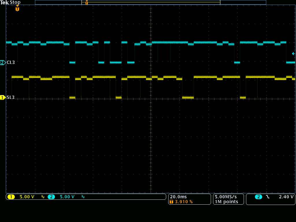 tek00040.png [ 23.05 KiB | Viewed 5001 times ]
Edit 7:
If I change the AVCC voltage, it has no effect on any of the 3 voltages of SL3/CL3.
Edit 8:
With AVCC connected and SL3/CL3 latched as inputs, if I momentarily disconnect M2 and reconnect it (i.e. trigger reset detection), SL3/CL3 unlock and start toggling again. Could it be that the MMC5, in general, gets held in reset mode by AVCC?
Edit 9:
Yes, theory in Edit 8 correct. PRG RAM +CE (the signal as pointed out by krzysiobal that reflects reset state) does reflect the latching of CL3/SL3.
Edit 10:
So, you are seeing where it can drive high or be an input, but it can not drive low. And once driven high, it can not be turned back into an input again until you cause a reset. The fact that you can drive high pretty much proves that it isn't a reset causing the problem like it was for me. But the fact that it gets stuck as an output, is different, and doesn't particularly sound broken if reset can still turn it back to an input. I like what you are saying about potential things going on with the PCB, that seems like the biggest difference between us at the moment.
Edit 11:
Something I didn't notice before, there are lots of little glitches where it drives low for a very short time in the scope shot, and it is always followed by driving high. I wonder what that is about?? I will zoom in on it tomorrow and also look at the glitch in comparison to M2 and CPU R/W, etc. The scope shot is actually
triggered on one of the glitches.

Quick question unrelated to the current bits: does /ROMCE additionally require that R/W be high? Or does it just pay attention to what banks are RAM vs ROM?
(I'm hoping to make a self-flashable cart)
MMC5-/ROMCE = CPU-/ROMSEL or CPU-R/WMMC5-/ROMCE = 0 when CPU-/ROMSEL = 0 and CPU-R/W= 0 and ROM is selected in current prg mode for current cpu address
If you want to make flash-cart:
* bend ROM-!CS pin 22 (which is tied to GND on MMC5 PCBs) and connect it to CPU-/ROMSEL (cart 44 pin)
* ROM-!OE pin 31 is already connected to MMC5-/ROMCE
* connect the /WE of Flash-ROM to CPU-R/W (cart 14 pin), so you gets:
Code:
action | ROM-!CS | ROM-!OE | ROM-!WE
write @ $8000-$ffff: | 0 | 1 | 0
read @ $8000-$ffff: | 0 | 0 | 1
outside $8000-$ffff: | 1 | x | x
---
Quote:
When you say that no current drop happens when writing to $5208, what to you mean? How do you measure that? Were you repeating my test method?
I write something (*) do $5207/$5208 and then just toggle M2 and measure the static average DC current supplied to MMC5
(*) something = for example $0/1/2/3/$40/$80/$c0 to $5207 and $00/$40/$80/$c0 to $5208. If there was internal short in the chip then it would drain lot more current when pin 97 and 98 are set to output different values, but for every of the combinations the current consumption is the same.
If outputs were broken, it would still allow me to bring them back as inputs by writing to $5207. I rather think the whole $5207 register is broken or my MMC5 does not have this functionality (maybe that's why no official game used it). PCB difference is rather irrelevant, without any chips, without battery and with the SL/CL jumper cut-out it is pretty same as yours.
I just found something very interesting CL3 that we have not seen before. In certain conditions, I have made CL3 = !(M2):
Attachment:
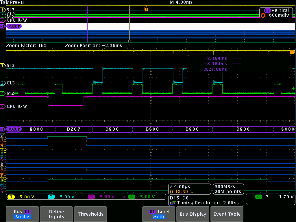 tek00046.png [ 36.54 KiB | Viewed 4920 times ]
I will narrow this down more but here are all of the conditions that I currently have (not sure which ones are relevant):
- Write a random byte to a random selection from this list of addresses:
$5000, $5002, $5003, $5004, $5006, $5007, $5010, $5015, $5100, $5101, $5102, $5103, $5104, $5105, $5106, $5107, $5113, $5114, $5115, $5116, $5117, $5120, $5121, $5122, $5123, $5124, $5125, $5126, $5127, $5128, $5129, $512A, $512B, $5130, $5200, $5201, $5202, $5203, $5204, $5205, $5206, $5207, $5208, $5209, $520A, $5800 - Exceptions: 1. Not including $5011. 2. If the address is $5800, always write $55
- Then after that, do 4 sequential reads from address $5800, which is where this CL3 behavior occurs.
- During the 4 reads, CL3 is the inverse of M2.
I still need to test:
- Read other addresses. What addresses can cause this? Shown in the scope shot is a read from $0000, which does not cause this, so it does seem to be address dependent.
- What values had been written to $5207 and $5208?
- Will I get this behavior from SL3 instead of CL3 if I write $AA instead of $55?
- Note that scope shot shows a write to $5207 just before this behavior.
Edit:
CL3 = !(M2) whenever reading from addresses in the range $5800-5BFF. Values checked: 57FF,
5800, 5801, 5A00, 5BFF, 5C00, D800, DBFF.
I found also that SL3 = !(M2) whenever
writing to $5800. Will verify range of SL3 writes and also try to figure out which values in $5207/5208 can cause this.
Ben Boldt wrote:
[*]Then after that, do 4 sequential reads from address $5800, which is where this CL3 behavior occurs.
[*]During the 4 reads, CL3 is the inverse of M2.
That sure sounds like it became a chip enable...
lidnariq wrote:
Ben Boldt wrote:
[*]Then after that, do 4 sequential reads from address $5800, which is where this CL3 behavior occurs.
[*]During the 4 reads, CL3 is the inverse of M2.
That sure sounds like it became a chip enable...
Yeah, it sounds sort of like a RAM RD / WR combo. Strange though with only a 1kbyte range, and in between the MMC5's registers and its own RAM...
More details:
Tested the write range for SL3, and it is the same range. To test the range, I wrote an $FF to different addresses and watched SL3. Then I tried writing different values to $5800. It doesn't make any difference if I write $FF, 00, 01, 02, or 03 when doing the write. I still have not worked on $5207/5208 but I am betting that writing $03 to $5207 is all it takes to put it into this mode.
Edit:
Yep, I power cycled, then wrote $03 to 5207, then wrote $03 to $5800 and triggered my scope on that one !(M2) pulse sent through on SL3.
In my MMC5 version writing anything to $5207 enabled this weird mode:
* During read cycle of any address in range $5800-$5bff: pin 97 goes low for duration of that cycle
* During write cycle of any address in range $5800-$5bff: pin 98 goes low for duration of that cycle
What if you cycle power, write $F0 to $5207, then $F0 to $5800? Do you get the pulse? Mine stays high when I do that, no pulse.
That is very interesting. Either we have different chip versions or parts of the logic are burned out in yours as you had originally suspected. I am not sure which is more likely. Between us, we have 3 L'Empereurs, we may have to try some more MMC5 chips with this. It will be interesting to see if you get an MMC5 or 5A in your L'Empereur. Both of mine had MMC5 letterless.
Either way, we get !(M2) out to SL3/CL3 when reading or writing in the address range $5800-$5BFF. That part is consistent. It seems like a way to expand the MMC5's internal RAM to 2x. What are the limitations of the existing internal RAM when used for the special PPU stuff that it can do? Are there any situations where doubling this RAM could be beneficial?
That can't be used for any fancy ... whatever external IC is attached can only be attached to one of the CPU's or PPU's data bus at any given time.
Given the values that Just Breed writes, it looks like they were using it for a CPU usage indicator.
And Just Breed doesn't initialize $5207 so those writes at $5800 are not externally vissible. Luckily, cause 97/98 are shorted.
I bet if any of those unknown five left MMC5 pins is /RD or /WR for the PPU-part of hypothetical dual-port RAM that could be externally connected.
lidnariq wrote:
That can't be used for any fancy ... whatever external IC is attached can only be attached to one of the CPU's or PPU's data bus at any given time.
Oh true, very good point.
lidnariq wrote:
Given the values that Just Breed writes, it looks like they were using it for a CPU usage indicator.
So far, we don't know any difference that depends on the value written to this address range. But the fact that they do 2 writes on entry and 1 write on exit would be easily measurable, you might be onto something.
I've just discovered that if both pins 81 & 82 are shorted to GND, it also puts MMC5 into reset state (which lasts until one of them goes high). This reset state is similar to the one caused by no action on M2 pin:
* EXRAM at $5c00-$5fff is turned off (it starts returning 00s), writing anything to $5104 does not stop it
* pins 97/98 becomes inputs
But there are also differences:
* PRG+CE is still active (logic 1)
krzysiobal wrote:
I've just discovered that if both pins 81 & 82 are shorted to GND, it also puts MMC5 into reset state (which lasts until one of them goes high). This reset state is similar to the one caused by no action on M2 pin:
* EXRAM at $5c00-$5fff is turned off (it starts returning 00s), writing anything to $5104 does not stop it
* pins 97/98 becomes inputs
But there are also differences:
* PRG+CE is still active (logic 1)
Very interesting. It has to be both 81 and 82 grounded at the same time? When you release them, does it always automatically get out of reset and start functioning again or do you ever have to trigger a gap in M2 to unlatch?
Do you have to release both of them to get out of reset? Can you GND both, and then release just 81 to get out for example, or does it wait for both to be released?
Unrelated question:
Are there any demo ROMs out there that get the MMC5 to do fancy stuff like vertical split screen with scrolling, etc? It would be interesting to probe the MMC5 while doing strange stuff like that.
I tried a lot of things today but didn't find anything new. I specifically looked for dual-port RAM /CEs or /WEs. I made a test where I wrote random data to 1 known writable register (selected randomly), then changed the PPU address bits randomly, and then changed the PPU /RD and /WR randomly. Then read 1 CPU address randomly, any address. Then loop. I never got any of the unknown pins to become outputs. I verified that my M2 gap never exceeded 10 usec in this test. I also individually drove low each unknown pin with a 500 ohm resistor to GND and read all of the other unknown pins. I found no effect from that. I did not try pins 81 and 82 at the same time or any other multiple pins at the same time. I also tried a 500 ohm to 2MHz function generator on each unknown pin, then set my scope to trigger on any frequency that fast. I probed all around with the test running, looking for 2MHz on the unknown pins, the PRG and CHR pins, etc. I never found 2MHz getting out anywhere.
Also during this test, I monitored CPU reads that caused the DAC to change value. I recorded 100 of such addresses with leaving all unknown pins floating. I found no statistical anomalies, which might have suggested a way to change the address range of DAC read mode. Not surprisingly, all changes in DAC value that I observed corresponded either to a write to $5011 or to a read in the range $8000-BFFF. Previous to this test, I did write non-zero incrementing data to all address $5800-5FFF.
No new findings but maybe some ideas. I took MMC5.97 (CL3), through a 500 ohm resistor, to each of the unknown pins (including SL3), then ran my test again, this time looking to see if the MMC5 drove the CPU data bus when reading from $5800. I also tried my random test with reads and writes outside of the range $5800-5BFF to see if any random register writes could affect the range of CL3/SL3. The range held true. This is a 1 kbyte range.
It is very strange to use CL3/SL3 to control RAM at $5800-5BFF, as $6000-6FFF already can only be used for RAM. If you were going to put 1k RAM at $5800, why on earth not just put it at $6000 and skip all this weird register business? That doesn't add up. Dual port RAM makes lots of sense, especially how the range $5800-5BFF is exactly the size of 1 nametable, but we seem to be missing some very elusive /CS /WE signals.
Riddle me this:
Code:
CPU Side PPU Side
CPU A0 A0 A0 PPU A0
CPU A1 A1 A1 PPU A1
CPU A2 A2 A2 PPU A2
CPU A3 A3 A3 PPU A3
CPU A4 A4 A4 PPU A4
CPU A5 A5 A5 PPU A5
CPU A6 A6 A6 PPU A6
CPU A7 A7 A7 PPU A7
CPU A8 A8 A8 PPU A8
CPU A9 A9 A9 PPU A9
CPU A10 A10 A10 CHR A10
CPU D0 D0 D0 PPU D0
CPU D1 D1 D1 PPU D1
CPU D2 D2 D2 PPU D2
CPU D3 D3 D3 PPU D3
CPU D4 D4 D4 PPU D4
CPU D5 D5 D5 PPU D5
CPU D6 D6 D6 PPU D6
CPU D7 D7 D7 PPU D7
GND /OE /OE PPU /A13
CL3 /CE /CE PPU /RD
SL3 /WE /WE PPU /WR
RAM +CE +CE +CE VCC
In this situation, we have 1 nametable mapped to CPU address range $5800-5BFF. Basically creating a different extended RAM for the other side of the vertical split screen. $5800-5BFF on one side of the split, $5C00-5FFF on the other side of the split. I guess that would play into the whole "ease of programming" thing because you could write to both sides the same way. But honestly it isn't really any different than writing to the PPU the normal way, maybe worse because now you don't have auto-increment PPU address, so I am not really sure where I am going with that idea.
Edit:
I realized on the way home that the PPU /A13 won't work, it will always enable the RAM, out of control of the MMC5... So that can't actually work that way.
Maybe my idea of additional dual-port ram was too extravagant. There is no register for switching fourth nametable nor pins for controlling /RD & /WE for the PPU side.
Knowing that in first mode you can use those two pins as general input/output (useful for driving any kind of two wire protocols like I2C - for EPROM memories), probably the second mode is just for utilizing them as /OE & /WE for some arbitrary external chip whose IO regs can be placed at $5800 (like extra audio chip - AY8910 or anything you can imagine). Or maybe this is remains of some debug device that was used in factory to test the chip.
Quote:
Very interesting. It has to be both 81 and 82 grounded at the same time? When you release them, does it always automatically get out of reset and start functioning again or do you ever have to trigger a gap in M2 to unlatch?
M2 was cycling all the time. I just grounded both of them (by 1k resistors) and it went into reset state. During reset state, it was not accepting commands (like writing to 02 to $5104 and reading from $5c00-$5fff still returnedzeros).
I had to disconnect one or two of those pins from GND and then write 02 to $5104 to make reads from EXRAm return non-zero things). No idea why this is two-pin reset. Maybe it is some comparator or place to connec two batteries and when they are grounded, MMC5 detects them as brown-out).
krzysiobal wrote:
Maybe my idea of additional dual-port ram was too extravagant. There is no register for switching fourth nametable nor pins for controlling /RD & /WE for the PPU side.
Knowing that in first mode you can use those two pins as general input/output (useful for driving any kind of two wire protocols like I2C - for EPROM memories), probably the second mode is just for utilizing them as /OE & /WE for some arbitrary external chip whose IO regs can be placed at $5800 (like extra audio chip - AY8910 or anything you can imagine). Or maybe this is remains of some debug device that was used in factory to test the chip.
Yes I suppose that sounds about right. We still don't really know why on earth they would have connected these pins together. That seems like a clue that we don't really understand, for some intended function. It has 2 different output modes that we know about. Maybe it has 2 different input modes somehow too. Set one as output, the other as input, and something could get enabled when reading or writing $5800... Seems like a strange way of doing things, but there must be some reason to connect those together. I can think of no other explanation than one being output and one being input. It can't be an ID thing with SL3/CL3 jumpers, or else there would be just a separate jumper to GND for each pin (you don't get more than 4 combos this weird way or anything). If you swap those jumpers as they are, one gets GND and the other floating. Close both, they both get GND. Those are not normal combinations, and that must be a clue. It persists on different boards too, it isn't just a weird quirk on 1 board.
I got my SMB 2J cart today. It doesn't work. Waaaa.... Black screen. I opened it and it does have the 3 big DIPs inside. However, the yellow case is one of the typical newer/thinner/cheaper ones. Will see if I can remove the W27C010 ROMs and dump them. If anything other than the glob is broken I will fix it, otherwise the ROMs will probably be transferred into an FC Wizardry if MMC3 is the right mapper.
I got the RAM chips today! Not tested yet. They appear pretty legit and have no signs of being soldered before. Will try putting one into my MMC5 socketed cart and using all the PRG-RAM lines we know about now!
Off topic (not really worthy of its own thread): With the SMB2J cart, I tested all connections of the PRG-ROM to the edge connector and all was good. Then I removed the EEPROMs and dumped them. I put an ines header set to MMC3 and put them into a file and it
did run in fceux. So I am thinking it is either the glob or the RAM chip. The ROM dump itself seems quite similar to loopy's MMC3 SMB2J but definitely has a small percentage of extra / different data. In areas where loopy's is all 00s (for example), this ROM has data there. Maybe it is an older revision of loopy's hack with unnecessary stuff still left in there? Anyway, will probably just scavenge the EEPROMs, reflash with loopy's latest, and hack up my Wizardry cart for this, which I got for just such a purpose. Anyone curious about this ROM dump should send me a PM.
My MMC5 cartridges finally arrived (my mistake - I ordered Suikoden, instead of Emperour). But the seller has 3 of them so I ordered all for tests. Unfortunately, all of them contains MMC5 (not MMC5A)
Strange thing is that none of them has registers at $5207, $5208, $5209, $520A ($5208 always return $FF - probably open BUS and does not reacts for writes for $5207). There is also no M2 clock timer at $5209-$520a (they return $FF too). I even cut CL3 jumper on one of them and it did not change anything.
I briefly analyzed my and botgod's database and it looks like MMC5 is newer and they started releasing it between 9129-9136 and Just Breed is the game which should contain it with highest probability.
Code:
8950AA089 MMC5 Suikoden: Tenmei no Chikai
8950AA105 MMC5 Suikoden: Tenmei no Chikai
8950AA108 MMC5 Nobunaga no Yabou: Sengoku Gunyuuden
9005AA048 MMC5 Uchuu Keibitai SDF
9006AA020 MMC5 Castlevania III: Dracula's Curse (USA)
9006AA029 MMC5 Bandit Kings of Ancient China
9008AA090 MMC5 Castlevania III: Dracula's Curse (USA)
9009AA046 MMC5 Suikoden: Tenmei no Chikai
9010AA017 MMC5 Suikoden: Tenmei no Chikai
9011AA045 MMC5 Sangokushi II
9026AA013 MMC5 Castlevania III: Dracula's Curse (USA)
9027AA024 MMC5 Ishin no Arashi
9032AA002 MMC5 Sangokushi II
9037AA033 MMC5 Sangokushi II
9042AA019 MMC5 Gunsight
9042AA025 MMC5 Nobunaga's Ambition II
9043AA001 MMC5 Daikoukai Jidai
9045AA018 MMC5 Castlevania III: Dracula's Curse (USA)
9046AA026 MMC5 Sangokushi II
9107AA013 MMC5 Romance of the Three Kingdoms II
9107AA024 MMC5 Romance of the Three Kingdoms II
9113AA024 MMC5 Shin 4 Nin Uchi Mahjong: Yakuman Tengoku
9114AA048 MMC5 L'Empereur (JPN)
9116AA003 MMC5 Laser Invasion
9117AA017 MMC5 Shin 4 Nin Uchi Mahjong: Yakuman Tengoku
9122AA019 MMC5 L'Empereur (USA)
9122AA020 MMC5 Nobunaga no Yabou: Bushou Fuuunroku
9122AA042 MMC5 Just Breed
9123AA002 MMC5 Castlevania III: Dracula's Curse (FRG)
9123AA012 MMC5 Castlevania III: Dracula's Curse (SCN)
9123AA043 MMC5 Gemfire
9126AA004 MMC5 Castlevania III: Dracula's Curse (SCN)
9126AA012 MMC5 Castlevania III: Dracula's Curse (SCN)
9126AA023 MMC5 Royal Blood
9128AA012 MMC5 Metal Slader Glory
9128AA013 MMC5 Uncharted Waters
9136BA026 MMC5A Just Breed
91378A013 MMC5A Just Breed
9141BA014 MMC5A Aoki Ookami to Shiroki Mejika: Genchou Hishi
9141BA020 MMC5A Just Breed
Oh very interesting, no wonder why these registers were missing in our original understanding of MMC5. You have motivated me to take a MMC5 letterless and put it on a breakout board and retry some of my old tests. It will take me some time to complete that; 100 wires takes a while... And probably delayed by the holidays but I will make it so I can swap my test setup between 5 and 5A easily. Especially I want to rerun my writable registers test.
It kind of begs the question - what do the CL3/SL3 pins do in MMC5 if not controlled by $5207/8?? Maybe they have a different function in this revision that makes sense to jumper them together.
I also want to revisit the scanline detection diagram with MMC5 letterless and confirm if it is the same or different. Thanks for opening the door to lots of new things to try krzysiobal!
Edit:
Now I also wonder about the PRG-RAM address bits you found in MMC5A, if they exist in MMC5.
After thinking a little more about this, I realized that the current spike write test only needs 25ish connections:
CPU D0-D7
CPU A0-A14
/ROMSEL
M2
Current probing / caps
So I put that together today and I tested the current spike when writing to each of these addresses:
$5000 - $5300 (each and every address in this range for MMC5, )
$5400, 5500, 5600, 5700
$57FF, 5800, 5801, 5802
$5BFF, 5C00, 5C01
MMC5 versus MMC5A, I confirmed that MMC5 is not reacting to writes to $5207, 5208, 5209, and 520A.
Also, it is not showing any reaction to writes in range $5800-5BFF.
Here is the data I recorded from MMC5 letterless, marking 9048AA033. I failed once again to inspect for any markings on the bottom of the chip while it was removed... My MMC5A has marking 9136BA033.
Code:
Addr MMC5 MMC5A
5000 9.44 8.56
5002 9.4 8.48
5003 12.12 12.36
5004 9.24 8.4
5006 9.16 8.4
5007 15.9 11.6
5010 8.84 7.96
5011 9.24 8.56
5015 8.56 7.76
5100 8.52 7.84
5101 8.36 7.64
5102 8.56 7.76
5103 8.56 7.8
5104 8.44 7.88
5105 8.44 8.12
5106 8.8 8
5107 8.52 7.64
5113 8.44 8
5114 8.44 8.08
5115 8.44 8.12
5116 8.56 8.04
5117 8.68 8.84
5120 8.96 8.68
5121 9.04 8.76
5122 9 8.68
5123 9 8.68
5124 9 8.68
5125 9.08 8.68
5126 8.96 8.64
5127 9.12 8.96
5128 8.84 8.52
5129 8.92 8.56
512A 8.88 8.4
512B 9.16 8.68
5130 8.52 8
5200 9.2 8.8
5201 8.88 8.32
5202 8.88 8.32
5203 8.68 8.12
5204 8.44 7.8
5205 8.8 8.24
5206 8.8 8.28
5207 7.8 8.68
5208 7.8 7.88
5209 7.8 11.2
520A 7.8 9.36
520B 7.8 7.2
I reran the test on both MMC5 and MMC5A because I made the test slightly different than before. In this test, I only write the value $00 -- I am no longer alternating between $00 and $FF writes. I am still toggling between writes to an invalid register and the register being tested, except now the invalid register is the same as the regsiter being tested, just with /ROMSEL inverted. Because the quantity of 1s vs 0s on the CPU address bus slightly affects the current drawn by the MMC5, this method helps keep things balanced and therefore easier to tell at a glance on the scope when the current spike got bigger or not.
In the table, MMC5 valid register spike is > 7.8, MMC5A valid register spike is > 7.2. All values should be considered relative to 7.8 or 7.2 respectively.
Edit:
I confirmed that PRG RAM A15 and A16
ARE functioning as prescribed on MMC5 letterless.
Edit 2:
The MMC5 DAC voltage still holds true to the MMC5A equation found earlier:
Voltage = [(DAC value / 255) * (0.4 * AVcc)] + (0.1 * AVcc)
Attachment:
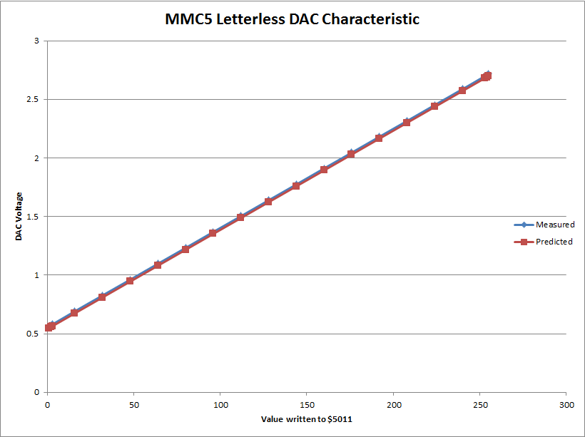 mmc5_letterless_dac_characteristic.png [ 15.39 KiB | Viewed 5013 times ]
Edit 3:
Nintendo HVC-ETROM-02 board beneath the MMC5 chip:
Attachment:
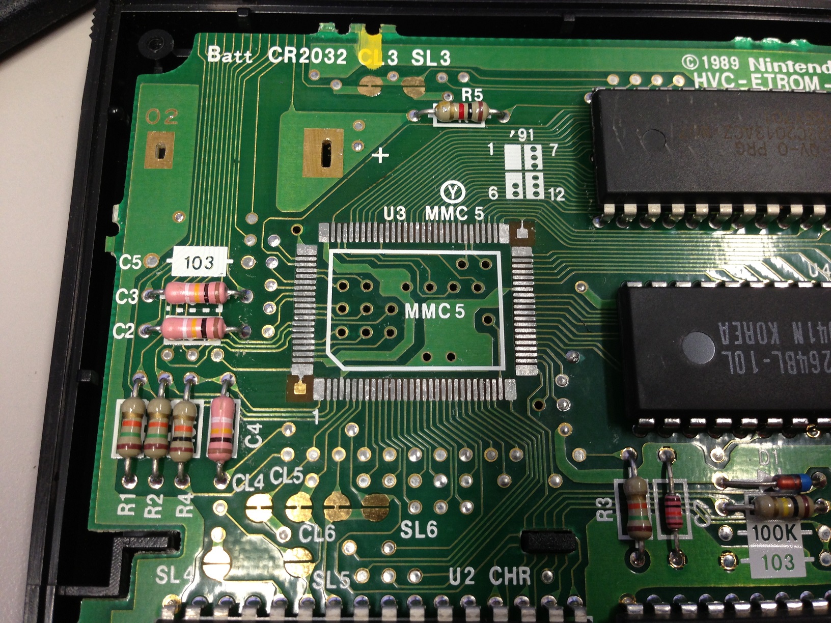 ETROM Board Beneath MMC5 Chip.jpg [ 791.03 KiB | Viewed 5004 times ]
Edit 4:
I have been reviewing this data tonight, and I found some interesting things when graphing it.
Attachment:
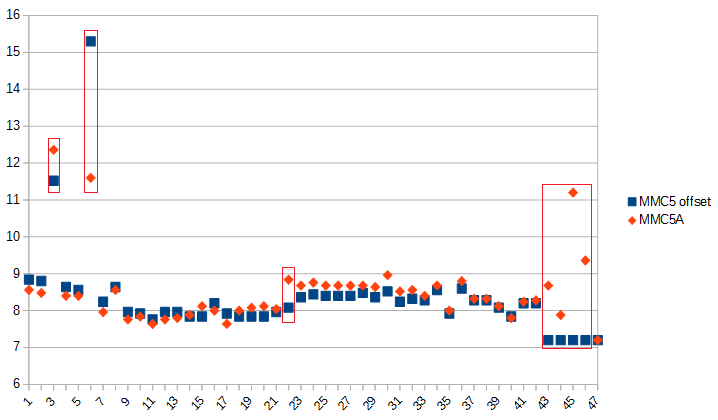 comparing writes.png [ 15.39 KiB | Viewed 4990 times ]
In this picture, I offset the values of the MMC5 to place them on top of MMC5A, making visual correlations easier. The first 2 items boxed correspond to $5003 and $5007. It seems they may have fixed something or took away something from $5007 (pulse 2 length counter load / timer high bits). In fact, I did have to change the vertical scale on my scope to make that measurement with the MMC5. It is not a typo. Bear in mind, the way I took these measurements, I had my microcontroller repeatedly write $00 to the register and measured with the scope running in real time. The way I did this was I modified my periodic idle read from address $0000 in the micro. Instead of reading, it does the write sequence. Because there is nothing else going on and I used a timer interrupt, the timing is extremely accurate and retriggers my scope very stable. Sorry for that tangent, but I thought I ought to explain how that way high point in the graph is real, and that this data is stable and repeatable.
Moving on to the 3rd box, this one corresponds to $5117, the ROM-only PRG bank. In MMC5, all PRG bank registers ($5113,4,5,6,7) all take relatively the same amount of current. In MMC5A, writing to $5117 has a larger effect than the others. This leads me to think that we should investigate CL3/SL3 in output 0 mode versus $5117 value when CPU address is reading from the range covered by bank $5117. Also to experiment with bit 7 in $5117 vs. CL3/SL3.
And the 4th box shows the now known-missing registers $5207,8,9,A.
There has been found a new commercial game for MMC5:
https://archive.org/details/simcity-nes Looks like you guys have something more to research.
Unfortunately, it looks like SimCity for the NES is "just" an ordinary ETEPROM board, with no modifications.
krzysiobal - I totally glazed over and missed where you found that the MMC5 is sniffing address $2000 and $2001 for 8x8 / 8x16 mode and just realized this when Lidnariq added it to the wiki recently. I went back and did my writable register test down there and I found a few more. All of these registers definitely are being sniffed:
$2000 (PPUCTRL) <- Both MMC5 and 5A
$2001 (PPUMASK) <- Both MMC5 and 5A
$2005 (PPUSCROLL) <- Both MMC5 and 5A
$2006 (PPUADDR) <- MMC5A ONLY
$4014 (OAMDMA) <- Both MMC5 and 5A
Note that $2007 (PPUDATA) does NOT appear to be writable on MMC5A. Very interesting.
I am thinking that it might be sniffing $2005 so as to keep track of its vertical split position during horizontal scrolling. Any ideas why it is listening to these other ones? And what improvement or bugfix in MMC5A causes it to be interested in PPUADDR but not PPUDATA? I suppose you only write to PPUADDR during v-blank; maybe it is a fail-safe scanline counter reset?
My first thought is it relates to the $2006-$2005-$2005-$2006 sequence (or whatever subset thereof was known to licensed devs).
Update:
I tried doing reads with this current spike test and in fact it does work for that too. It revealed that MMC5 and 5A are both sniffing reads from $2002 (PPUSTATUS). Confirmed not sniffing reads or writes from $2007 on MMC5 or 5A. This test does not work for the known $FFFA/B sniffs that reset the scanline counting state machine, as expected because that is known to be an asynchronous operation and this test only finds M2 edge triggered reads/writes.
New list of known sniffs:
Code:
Addr | Name | R/W | Registration | MMC5 Revisions | Purpose
------+------------------+-------+--------------+-------------------------+--------------------
$2000 | PPUCTRL | WRITE | M2 Rising | Both MMC5 and 5A | 8x16 Mode Enable 1
$2001 | PPUMASK | WRITE | M2 Rising | Both MMC5 and 5A | 8x16 Mode Enable 2
$2002 | PPUSTATUS | READ | M2 Rising | Both MMC5 and 5A | (unknown/unconfirmed)
$2005 | PPUSCROLL | WRITE | M2 Rising | Both MMC5 and 5A | (unknown/unconfirmed)
$2006 | PPUADDR | WRITE | M2 Rising | MMC5A *ONLY* | (unknown/unconfirmed)
$4014 | OAMDMA | WRITE | M2 Rising | Both MMC5 and 5A | (unknown/unconfirmed)
$FFFA | NMI Vector Low | READ | Asynchronous | only confirmed on MMC5A | Triggers reset of scanline counter
$FFFB | NMI Vector Hi | READ | Asynchronous | only confirmed on MMC5A | Triggers reset of scanline counter
$FFFA is the NMI vector...
lidnariq wrote:
$FFFA is the NMI vector...
Oh duh, my bad. I will edit that post.
tepples wrote:
My first thought is it relates to the $2006-$2005-$2005-$2006 sequence (or whatever subset thereof was known to licensed devs).
I wouldn't assume licensed devs knew anything better than what was done in SMB3, namely: 6/6/5/5 on the title screen; 6/6/6/6/disable rendering/6/6/enable rendering/5/5 during gameplay.
Ben Boldt wrote:
lidnariq wrote:
$FFFA is the NMI vector...
Oh duh, my bad. I will edit that post.
It kind of begs the question - does reading the reset vector reset the MMC5? Do we know that already? I don't remember now.
Edit:
I tested MMC5A by removing and reconnecting the AVCC connection a few times until I got it into latched-reset mode, demonstrated by PRG-RAM +CE held low even with M2 toggling. I did repeated reads to all addresses $FFF0-FFFF and it did not unlatch the reset. I think that makes it unlikely that reading the reset vector triggers the MMC5 reset.
I don't understand how is MMC5 reacting to $2002 reads. I understand how it can snoop writes to $2000, $2001, $2005 and $2006 for internal operation. What I don't understand is, does the MMC5
a) Fill the unused low 5 bits of $2002 with some more information
or
b) Trigger some internal operation on $2002 reads, possibly snooping the upper 3 bits showing up on the data line and using them somehow internally ?
Or something else entirely ?
The MMC5 cannot fill bits 4-0 of $2002 with other information because the PPU is already driving bits 4-0 based on the value of
PPUGenLatch, the last value read from or written to $2000-$3FFF.
B; the PPU still drives the lower 5 bits (with garbage) and competing would invoke a bus conflict.
But I also wouldn't be surprised if the designer had hoped to add extra status bits there (i.e. "A") and it had to be removed.
Wow, I didn't know it wasn't open bus, but buffered garbage. My bad, apologizes.
Could we please include a verbal description of the two "state machine" diagrams on the wiki page? I find it difficult to understand them. It is also not clear on how the MMC5 detects whether it should switch in the background or sprite banks in 8x16 sprite mode.
NewRisingSun wrote:
Could we please include a verbal description of the two "state machine" diagrams on the wiki page? I find it difficult to understand them. It is also not clear on how the MMC5 detects whether it should switch in the background or sprite banks in 8x16 sprite mode.
For the scanline counting state diagram, there are some comments in dotted line boxes on the right side of the diagram, which was intended to explain it. I am a little bit puzzled where I could improve it. Are you understanding parts of it and getting stuck, or is it more of a matter of not knowing where to start? If you are getting stuck, please explain the parts that you do understand and then where you get stuck, and I will do what I can to improve it. Otherwise, I will think about how to make it easier to approach.
What does it mean if one state's arrow points to itself? Are the text fields next to the arrows the conditions that must be fulfilled for the arrow to apply, or a description of what happens during the transition from one state to the next? If the former, why is "Addr Match" inside a state rectangle if it is also a condition? Why designate step 3 as the initial state, which is highly unintuitive? Why put "/RD goes low" into every text field, even though it just seems to clock the "state machine"? What does the sentence "It gates transition of the other state machine from step 3 to step 0" mean? What does it mean to "gate transition"? And who is "it"?
Nowhere is it make explicit that the upper "state machine" basically detects three M2 cycles without a PPU read, and that the lower "state machine" detects three reads from the same PPU address in the $2xxx range. It may be "obvious" to somebody who understands state diagrams, but is nebulous to those who don't. I question the value of state diagrams in general --- to me, they seem like shoehorning a simple concept into a complex abstraction for the hell of it, though in your case, I think I can comprehend why they would seem to be a good representation when starting from the point of view of somebody who feeds various inputs into a "black box" of a chip and then checks the output.
I prefer to start with a precisely- and concisely-written verbal theory of operation, optionally followed by a piece of pseudo-code that clears up the details. That is the way it is done in most other nesdev wiki articles on complex subjects such as PPU Sprite Evaluation. I can offer to draft such a thing, and you can then correct it.
And again, the wiki article still lacks an explanation of how the MMC5 detects whether it should use the background or sprite banks when 8x16 mode is active.
NewRisingSun wrote:
It may be "obvious" to somebody who understands state diagrams, but is nebulous to those who don't. I question the value of state diagrams in general --- to me, they seem like shoehorning a simple concept into a complex abstraction for the hell of it, though in your case, I think I can comprehend why they would seem to be a good representation when starting from the point of view of somebody who feeds various inputs into a "black box" of a chip and then checks the output.
Thanks for the feedback, I will do what I can to improve it. I am sorry if I suggested that understanding this diagram should be obvious. The scanline counter is pretty complex, and the way it works can take lots of different paths depending on the situation. A lot of other stuff inside the NES and mappers works like: if X, do Y, otherwise Z, lending itself well to a text/pseudocode description. But in this case there are a lot of interactions. The state diagram captures every known detail, which may be overwhelming or more information than is necessary for most people. I will take some time and work on this with your feedback. I would be open to working with you starting a written draft on this.
Okay! Here's my first serve:
--
The MMC5 detects scanlines by looking for three consecutive PPU reads from the same address in the $2xxx PPU range, which are performed by the PPU at the end of every rendered scanline
(cycles 337-340). If the "in-frame" flag was clear at this point, it is set, and the scanline counter is reset to zero; if it was already set, the scanline counter is increased, then compared against the value written to $5203. If they match, the "irq pending" flag is set. This implies that a $5203 value of $00 will never generate an IRQ, because the scanline counter is increased from $00 to $01
before it is compared against the $5203 value.
The "in-frame" flag is cleared either when ...
- ... the PPU is no longer rendering, i.e. three CPU cycles pass without a PPU read having occurred (PPU /RD has not been low during the last three M2 rises), or
- ... a non-maskable interrupt is invoked, i.e. CPU addresses $FFFA or $FFFB are read from, or
- ... the user program disables rendering, i.e. CPU address $2001 is written to with bits 3 and 4 clear.
This means in pseudo-code:
On every PPU read ("/RD falling edge"):
Code:
if address >= $2000 and address <= $2FFF and address == lastAddress
matchCount := matchCount +1
if matchCount == 2 ; will be 2 on the *third* read because of the previous address == lastAddress condition
if inFrame == false
inFrame := true
scanline := 0
else
scanline := scanline +1
if scanline == [$5203]
irqPending := true
else
matchCount := 0
lastAddress := address
ppuIsReading := true
On every CPU cycle ("M2 rising edge"):
Code:
if ppuIsReading
idleCount := 0
else
idleCount := idleCount +1
if idleCount == 3
inFrame := false
ppuIsReading := false
On every CPU write:
Code:
if address == $2001 and (value & $18) == 0
inFrame := false
On every CPU read:
Code:
if address == $FFFA or address == $FFFB
inFrame := false
---
This is probably a bit too simplistic, but it will be valuable to identify the scenarios in which this simplified description is not correct, and of course if I have greatly misunderstood something.
Sorry, I wrote this before I saw your post. We should take some time to review both of our descriptions and try to take the best of both / combine them. Here is what I wrote:
The bottom state machine is used to "unlock" the top state machine. At power-on, the bottom state machine initializes as unlocked. When unlocked, it remains unlocked for any subsequent reads from addresses in the range $2000-2FFF, matching or not. It becomes locked any time that the PPU reads from an address that is outside the range $2000-2FFF. Once locked, the PPU must read from the same address 3 times in a row in the range $2000-2FFF in order to unlock again.
The top state machine sets and clears the "in frame" status bit, which increments the scanline counter, which can be set up to generate scanline interrupts. At power-on, the top state machine initializes as "not in frame". Any time that the top state machine is "not in frame", and the PPU does any read while the bottom state machine is unlocked, "in frame" becomes set and the scanline counter increments. Once the top state machine is "in frame", 3 sequential M2 rising edges without the PPU doing any reads will go back to "not in frame". The top state machine will go directly to "not in frame" whenever the CPU reads from address $FFFA or $FFFB (i.e. the V-Blank interrupt vector). This does not lock, unlock, or change the bottom state machine in any way.
Edit:
To clarify 1 thing about state diagrams that you mentioned -- when a state has an arrow that goes back to itself. These exist in the diagram simply to show something that has no effect. It is showing that when you do whatever this arrow says, it does not take you to a different state. I will spend some time tonight reviewing what you wrote (I have not had time today yet) and I will think more about how the state machine behaves specifically in the context of the things that the PPU and CPU actually do.
Here is some C pseudo-code, but still not considering the context of what the PPU and CPU actually can and can't do, which may provide some shortcuts or better explanations:
Code:
typedef enum
{
NOT_IN_FRAME,
IN_FRAME
}in_frame_e;
static int m2_rising_edge_count = 3; // Value 0,1,2 = In Frame. Value 3 = Not in frame. Power-on value = 3.
static int ppu_rd_falling_edge_count = 3; // Value 0,1,2 = Locked. Value 3 = Unlocked. Power-on value = 3.
static int scanline_counter = 0;
in_frame_e is_in_frame( void )
{
if( 3 == m2_rising_edge_count )
{
return NOT_IN_FRAME;
}
else
{
return IN_FRAME;
}
}
void m2_rising_edge_occured( void )
{
if( m2_rising_edge_count < 2 ) // In Frame. 0 -> 1, 1 -> 2
{
m2_rising_edge_count++;
}
else // On the 3rd M2 rising edge:
{
// Not in frame
}
}
void ppu_read_detected( uint16_t ppu_addr ) // i.e. PPU /RD falling edge
{
static uint16_t ppu_addr_prev;
// FIRST, update the top state machine
if( 3 == m2_rising_edge_count ) // If not in frame:
{
if( 3 == ppu_rd_falling_edge_count ) // If unlocked:
{
m2_rising_edge_count = 0; // ** Become In frame. **
scanline_counter++;
// Check for interrupt, etc.
}
else
{
// It was locked, stay "not in frame"
}
}
else // If already in frame:
{
// Reset m2 counter:
m2_rising_edge_count = 0; // Remain in frame.
}
// NEXT, update bottom state machine.
// Note that updating M2 can lock it, so this must be done after updating the top state machine.
if( 0 == ppu_rd_falling_edge_count ) // Locked (count 0). PPU address RANGE Check.
{
if( (ppu_addr >= 0x2000) && (ppu_addr < 0x3000) )
{
ppu_rd_falling_edge_count++;
ppu_addr_prev = ppu_addr;
}
}
else if( ppu_rd_falling_edge_count < 3 ) // Locked (count 1, 2). PPU address MATCH check.
{
if( ppu_addr == ppu_addr_prev )
{
ppu_rd_falling_edge_count++;
}
else
{
ppu_rd_falling_edge_count = 0;
}
}
else // Unlocked (count 3). PPU address RANGE Check to stay unlocked.
{
if( (ppu_addr < 0x2000) || (ppu_addr >= 0x3000) )
{
ppu_rd_falling_edge_count = 0; // Lock it.
}
// else stay unlocked.
}
}
void cpu_read_vblank_interrupt_vector( void )
{
m2_rising_edge_count = 3; // Not in frame
// Theoretically: (I didn't ever test/verify this)
scanline_counter = 0;
}
I am working through the frame timing diagram here:
https://wiki.nesdev.com/w/index.php/PPU_renderingThis is boxes 0 to 16, showing state machine state (x,y), where x is the top state machine state 0,1,2,3 (0,1,2 = in frame, 3 = not in frame), and y is the bottom one (0,1,2 = locked, 3 = unlocked). Please anyone reading, correct me if my PPU sequences are not correct. I am assuming that PPU /RD goes low only on the 2nd cycle of each pair of PPU cycles for example. I am still not very familiar with the PPU, which has lent itself to the issues with my description that NewRisingSun is trying to help fix.
Code:
Initial power-on state = (3,3: not in frame, unlocked)
M2 Falls
(0): Idle Cycle
/RD: Stays Hi (?)
-----------------------------------------------------
M2 Rises => (3,3: not in frame, unlocked)
M2 Falls
(1): NT Address ($2000-2FFF)
/RD Stays Hi
M2 Rises with /RD hi => (3,3: not in frame, unlocked)
M2 Falls
(2): NT Data ($2000-2FFF)
/RD Falls => (0,3: **IN FRAME** 0, unlocked)
M2 Rises with /RD low
M2 Falls
(3): AT Address ($2000-2FFF)
/RD Stays Hi
M2 Rises with /RD hi => (1,3: in frame 1, unlocked)
M2 Falls
(4): AT Data ($2000-2FFF)
/RD Falls => (0,3: in frame 0, unlocked)
M2 Rises with /RD low
M2 Falls
(5): Low BG Address ($0000-1FFF)
/RD Stays Hi
M2 Rises with /RD hi => (1,3: in frame 1, unlocked)
M2 Falls
(6): Low BG Data ($0000-1FFF)
/RD Falls => (0,0: in frame 0, **LOCKED** 0)
M2 Rises with /RD low
M2 Falls
(7): Hi BG Address ($0000-1FFF)
/RD Stays Hi
M2 Rises with /RD hi => (1,0: in frame 1, locked 0)
M2 Falls
(8): Hi BG Data ($0000-1FFF)
/RD Falls => (0,0: in frame 0, locked 0)
M2 Rises with /RD low
-----------------------------------------------------
M2 Falls
(9): NT Address ($2000-2FFF)
/RD Stays Hi
M2 Rises with /RD hi => (1,0: in frame 1, locked 0)
M2 Falls
(10): NT Data ($2000-2FFF)
/RD Falls => (0,1: in frame 0, locked 1)
M2 Rises with /RD low
M2 Falls
(11): AT Address ($2000-2FFF)
/RD Stays Hi
M2 Rises with /RD hi => (1,1: in frame 1, locked 1)
M2 Falls
(12): AT Data ($2000-2FFF)
/RD Falls => (0,2: in frame 0, locked 2)
M2 Rises with /RD low
M2 Falls
(13): Low BG Address ($0000-1FFF)
/RD Stays Hi
M2 Rises with /RD hi => (1,2: in frame 1, locked 2)
M2 Falls
(14): Low BG Data ($0000-1FFF)
/RD Falls => (0,0: in frame 0, locked 0)
M2 Rises with /RD low
M2 Falls
(15): Hi BG Address ($0000-1FFF)
/RD Stays Hi
M2 Rises with /RD hi => (1,0: in frame 1, locked 0)
M2 Falls
(16): Hi BG Data ($0000-1FFF)
/RD Falls => (0,0: in frame 0, locked 0)
M2 Rises with /RD low
What this is driving towards is to map out exactly how the state diagram interfaces with the fetch patterns of the PPU, and from there we can get a very clear big picture and be able to describe in english the actual intentions of how this is working.
Edit:
I fixed a couple of errors in the PPU sequence.
Edit 2:
So, it repeats 9-16 for the whole range 9-256. Then in the range 257-320, it quickly becomes not-in-frame because there are M2 cycles and no PPU /RD cycles. Then in range 321-336, it stays not-in-frame due to being locked and no 3-in-a-row matching PPU address reads. Then in range 337-340, looping to 0-2, there are 3 matching NT PPU reads in a row, which unlocks, and then on 3 (PPU AT read) it becomes in-frame. Does this sound correct? This is really a mess but I think I am starting to understand it, which is probably a good step toward building a more concise explanation here.
Ben Boldt wrote:
Then in the range 257-320, it quickly becomes not-in-frame because there are M2 cycles and no PPU /RD cycles.
No, the PPU fetches throughout horizontal blanking; it just fetches always from the same NT address (interspersed with CHR fetches, so no scanline detector trigger here), which can be a means of detecting SPR from BG.
I have implemented the scanline and in-frame detector according to my simple state-machine-less description. I assume that the MMC5 detects SPR by checking, for every in-frame nametable (not attribute table!) access whether it matches the previous address, and if so, assume SPR, otherwise switch to BG. All of this works almost perfectly except for the very first rendered scanline's first two tiles being wrong, and the IRQ being generated one cycle or so too late, causing a jumpy split in Metal Slader Glory. The latter may well be due to Nintendulator's PPU fetch emulation itself being slightly off by a cycle or two. I am not sure how the first scanline's first two tiles could
not be garbage, given that the three-reads-from-the-same-address only occurs after their data has been fetched.
We already know that the MMC5 keeps count of which nametable/pattern table fetch is happening, to implement 8x16 sprite mode (
see Krzysiobal's test) and left-and-right split mode.
Previous evidence has found that it's not always the exact same dummy nametable fetch during sprite pattern fetches; it kinda appears like it might be some kind of open bus value internally.
All right, detect BG/SPR from the same currentTileNumber variable as the split screen.
I will later do a raw video capture, using a card/software that accurately samples scanline 0, to see if there is any garbage in the top left corner in Just Breed.
NewRisingSun wrote:
No, the PPU fetches throughout horizontal blanking; it just fetches always from the same NT address (interspersed with CHR fetches, so no scanline detector trigger here), which can be a means of detecting SPR from BG.
Could you provide a cycle-by-cycle example of what the PPU does during this time -- or point me to the right place if this is described somewhere? Is it predictable and always follows a certain pattern? I would like to understand this. Also, was I correct with how M2 synchronizes with PPU /RD in my example?
Ultimately, I would like to simulate the full PPU rendering diagram with my state machines visually updating beside it. For me, seeing it shown visually like that will help my understanding a lot. I want to show the rendering diagram in a window, and have a button that steps through and shows each step what is happening. From there I can describe the actual behavior better, and you guys can check it out and show me my mistakes and wrong assumptions that I will definitely make. It may also point to problems in my state diagrams and especially undiscovered paths.
I would like to say something simple and general like "any 3 PPU reads from the same address in range $2000-3FFF sets the in frame bit". We know that there are conditions where it will set "in frame" from just 1 or 2 PPU reads, but we don't know if there are realistic PPU sequences to actually ever get into those conditions or not, so they might matter or might not. That really is why we are still stuck with such a complicated diagram/explanation.
I will work on building a simulator for this.
Ben Boldt wrote:
Could you provide a cycle-by-cycle example of what the PPU does during this time -- or point me to the right place if this is described somewhere?
https://wiki.nesdev.com/w/index.php/Fil ... timing.pngQuote:
Is it predictable and always follows a certain pattern?
Mostly. Nametable/attribute table fetches during sprite sliver fetches appear to be unpredictable garbage.
Why, right on the same wiki page, in the text above that frame timing diagram. That frame diagram is kind of hard to understand. I would even go as far as saying that it's wrong. And the fact that it gave you the idea that the PPU does not read anything from cycle 258-320 kind of underlines that it's wrong. (You can tell that I am easily annoyed by what I consider bad visualizations.
)
I am not quite sure though why we need a simulator to write a few lines of text. That seems more like complicating things instead of simplifying them.
I have just captured the video output of
Just Breed, running my cartridge of the game on the Sharp Twin Famicom AN-505BK, using my custom setup that allows me to capture the raw NTSC output before any capture card or software messes with it. This is necessary because most capturing software by default crops the very first NTSC scanline. And the result:
Attachment:
 JustBreed1.png [ 66.14 KiB | Viewed 3089 times ]
Attachment:
 JustBreed2.png [ 273.95 KiB | Viewed 3089 times ]
Note the two garbage lines in the top left corner. They are not seen in non-MMC5 games using this capturing setup.
Yes, the MMC5
does output garbage tiles for the first two tiles on scanline 0 in this game, because the "in-frame" flag only gets set
after the two garbage nametable fetches on the pre-render scanline, which
follow the fetches for tiles 0 and 1, and the "in-frame" flag affects which CHR banks are mapped. This might be considered a test for any emulator that implements the scanline/in-frame detector.
I have also attached my raw captures so nobody can say that I messed with the .png files to create a desired result or something.
Edit: Oh, and the slightly jumpy split in
Metal Slader Glory seems to occur on real hardware as well (
https://youtu.be/jMUobWk4Qbg?t=38).
Edit 2: I forgot that Just Breed disables rendering in the left eight pixels via $2001. This means that there are actually
three garbage tiles, meaning that the CHR bank switch that is triggered by setting the in-frame flag does not occur until after the third tile at cycle 1 has been fetched.
NewRisingSun wrote:
I am not quite sure though why we need a simulator to write a few lines of text. That seems more like complicating things instead of simplifying them.
I think I made it sound more fancy than it really is.
Attachment:
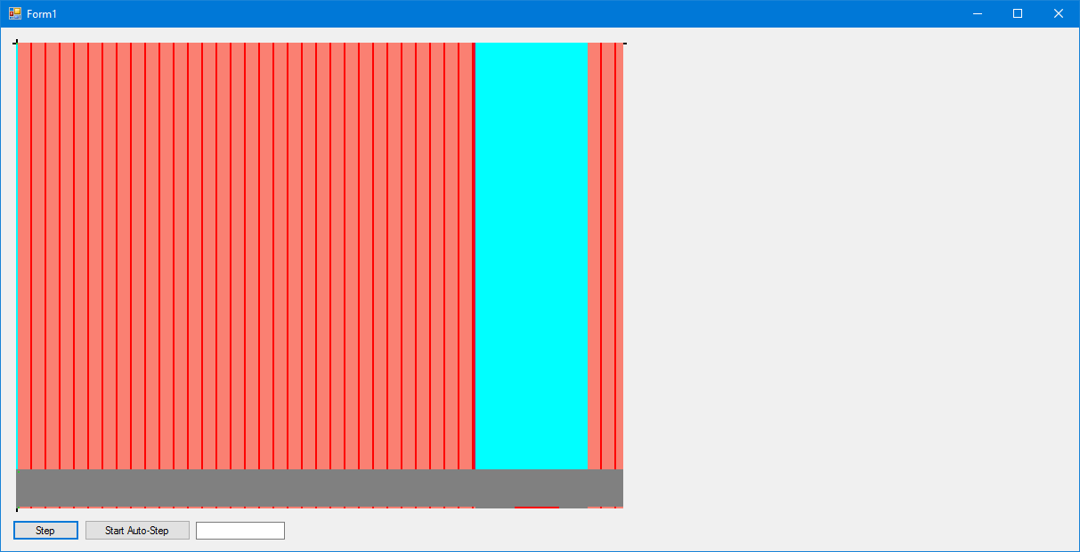 ppu_sim.png [ 17.23 KiB | Viewed 3059 times ]
I guess I kind of need it for my own understanding. I feel like I have very little grasp on the PPU's operations and this would make it easier. It will not be a very complicated simulation. I already did most of it; it basically it shows all of the boxes from the Wiki's timing diagram and it blinks the box that you are on. It lets you step PPU cycles and also has a timer to auto-step PPU cycles so you can just watch it. I will see if I can get it finished tonight.
Okay, but keep in mind that the timing diagram is wrong from cycles 258-320, as mentioned earlier.
Edit: Or maybe it's not wrong at all, just confusing as hell. Instead, the two top graphs apparently are supposed to describe background rendering only, and the bottom graph is supposed to describe the sprite rendering? My god, how confusing. That's why I never use diagrams.
NewRisingSun wrote:
Okay, but keep in mind that the timing diagram is wrong from cycles 258-320, as mentioned earlier.
Edit: Or maybe it's not wrong at all, just confusing as hell. Instead, the two top graphs apparently are supposed to describe background rendering only, and the bottom graph is supposed to describe the sprite rendering? My god, how confusing. That's why I never use diagrams.
Well, for better or for worse, we have all sorts of different strange people that like NES and some of them are completely lost without diagrams.
I got some things going with the simulator thing. It does scanlines 0-239 but still does not simulate the cyan areas. As soon as it gets to the cyan area, it sets it to "not in frame" and locked. Please have a look and see if you can find any problems. I will still need to think about the cyan area, I do not understand it yet.
The attachment is a MS Visual studio project. You can either open it in Visual Studio to run it, or you can run the pre-built EXE if you dig down to:
\PPU MMC5 Sim\PPU MMC5 Sim\bin\Debug\
Is there any place during scanlines 0 - 239 where there could be 3 M2 cycles without any PPU read cycles? I am really stuck because it looks to me like it reads on every single even cycle until scanline 240. During the cyan sprite area, it has the gargabe NT and AT cycles but I think those are reads even though they are garbage. PPU /RD would go low, garbage or not.
You're correct, every scanline is 171 pixels of /RD high and 170 pixels of /RD low. The one stutter is at the "idle" pixel on the diagram.
lidnariq wrote:
You're correct, every scanline is 171 pixels of /RD high and 170 pixels of /RD low. The one stutter is at the "idle" pixel on the diagram.
I think that idle cycle is the key. Here is how I think these signals work:
Attachment:
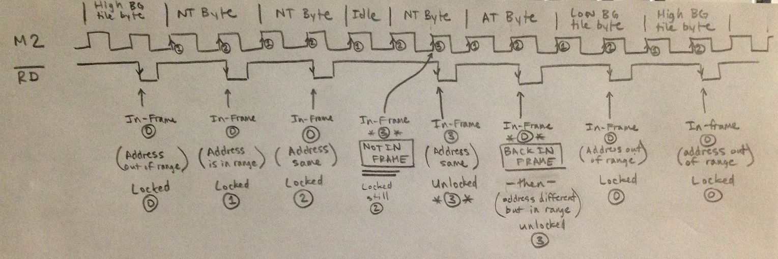 timing.jpg [ 298.85 KiB | Viewed 3005 times ]
If I understand this right, it looks like the in-frame bit gets cleared for only a very short time after the idle cycle during each scanline 0-239. Then presumably for scanlines 240-260, in-frame remains cleared the whole time.
Based on this, I would say that the scanline counter increments and IRQ generated at the first AT byte read of each scanline. There may be corner conditions for the first scanline and pre-render scanline where my simulator can come back to help us.
It seems intuitive that the scanline counter would increment, leading to IRQ, each time that "in-frame" status bit gets set to 1. But to my knowledge, we have never confirmed that isn't actually happening when the status bit gets set to 0. If my drawing is correct, it might make more sense to increment and IRQ based on when the status bit becomes 0. I will see if I can check that soon, but I am staying home tomorrow due to extreme cold temperatures.
Ben Boldt wrote:
Based on this, I would say that the scanline counter increments
No, we already know that. It's from when the PPU fetches the same exact address from the upper half of the space three times in a row. Everything else comes from that...
There's no good way to detect the idle pixel without a much faster clock than M2. (Incidentally, the idle pixel is approximately right on the left edge of the visible frame. It happens after the first two slivers of background tile data have been fetched)
... why do you think the MMC5 goes "out of frame" every scanline?
lidnariq wrote:
from the upper half of the space three times in a row.
I am sorry, I just do not follow. What do you mean by upper half? Could you take a screenshot of the PPU diagram and circle the spot where this happens?
lidnariq wrote:
... why do you think the MMC5 goes "out of frame" every scanline?
It was my understanding that the scanline counter increments
each time that the 'in frame' status bit toggles and that someone had not picked the best name for this status bit. My state diagram explains specifically the operation of the 'in frame' status bit. I created the diagram by looking at the status bit, not by setting up IRQs and waiting for them to happen due to the scanline counter incrementing. In hindsight, and to your point, I never tested or confirmed any connection between the status bit and the IRQ. Maybe there isn't any?? I was so sure of that...
lidnariq wrote:
why do you think the MMC5 goes "out of frame" every scanline?
He wrote that he got that idea from that confusing PPU timing diagram on the wiki, because of those large blue-shaded areas in that diagram.
Ben Boldt wrote:
Please have a look and see if you can find any problems.
Sorry, but no. All I wanted is a short text description and pseudo-code of those two state diagrams, simplified from the abstract "state machine" terminology. Now I am looking at those same diagrams, plus a confusing PPU timing diagram, plus an MS Visio project of a PPU simulator. That is exactly what I did not want.
I have my MMC5 emulation working nice and well based on my limited understanding of those state diagrams, which have laid out in my pseudo-code, and it has turned out to be correct enough to run all games well, both in terms of IRQ, scanline split, and even scanline-0 graphical artifacts. That is all I needed.
NewRisingSun wrote:
lidnariq wrote:
why do you think the MMC5 goes "out of frame" every scanline?
He wrote that he got that idea from that confusing PPU timing diagram on the wiki, because of those large blue-shaded areas in that diagram.
That actually is not where I got the idea, and I am not yet sure that it is incorrect.
NewRisingSun wrote:
Ben Boldt wrote:
Please have a look and see if you can find any problems.
Sorry, but no. All I wanted is a short text description and pseudo-code of those two state diagrams, simplified from the abstract "state machine" terminology. Now I am looking at those same diagrams, plus a confusing PPU timing diagram, plus an MS Visio project of a PPU simulator. That is exactly what I did not want.
I have my MMC5 emulation working nice and well based on my limited understanding of those state diagrams, which have laid out in my pseudo-code, and it has turned out to be correct enough to run all games well, both in terms of IRQ, scanline split, and even scanline-0 graphical artifacts. That is all I needed.
I am actually being a little bit selfish here NewRisingSun, I am doing this also very much for my own understanding, which is very lacking at the moment. I think I am looking for a complete explanation that exceeds what is necessary for what you are doing, and then working back from that proven full understanding to the simpler type of explanation you are looking for, instead of taking liberties and jumping directly to a simple "good-enough" solution. Our goals are different, and I would not ask to drag you through my lengthy process if you aren't interested.
Also, I am not sure how M2 synchronizes with PPU /RD. Does my hand-drawn picture look correct how these are synced up? I will check it eventually with my scope.
Also, lidnariq - you refer to each PPU cycle as a 'pixel', it seems that each cycle is a row of 8 1-bit pixels. Is this what you meant or is my understanding incorrect on this?
Ben Boldt wrote:
That actually is not where I got the idea
You
wrote: "I am working through the frame timing diagram here:", followed by: "Then in the range 257-320, it quickly becomes not-in-frame because there are M2 cycles and no PPU /RD cycles." No. There are PPU /RD cycles throughout that area, as shown by the lower part of that diagram. Your conclusion that the PPU goes out-of-frame each scanline is wrong as a consequence. The PPU never stops reading until the end of scanline 239, or if the software disables rendering by writing to $2001.
Ben Boldt wrote:
instead of taking liberties and jumping directly to a simple "good-enough" solution
I am not taking any "liberties" or "jumping to solutions". I make things as simple as possible, and as complex as necessary.
Ben Boldt wrote:
I am sorry, I just do not follow. What do you mean by upper half? Could you take a screenshot of the PPU diagram and circle the spot where this happens?
We already know that the MMC5 counts its IRQ counter if
* The PPU fetches address X, where X ≥ $2000
* The PPU fetches address X again
* The PPU fetches address X a third time
Only after the third step is this sufficient to clock the IRQ counter.
We've known the horizontal timing for more than a decade:
viewtopic.php?p=12379#p12379Drag wrote a test that took advantage of predictable peculiarities of the PPU's fetch sequence to clock the MMC5 IRQ an extra scanline:
viewtopic.php?f=9&t=7653
NewRisingSun wrote:
Ben Boldt wrote:
That actually is not where I got the idea
You
wrote: "I am working through the frame timing diagram here:", followed by: "Then in the range 257-320, it quickly becomes not-in-frame because there are M2 cycles and no PPU /RD cycles." No. There are PPU /RD cycles throughout that area, as shown by the lower part of that diagram. Your conclusion that the PPU goes out-of-frame each scanline is wrong as a consequence. The PPU never stops reading until the end of scanline 239, or if the software disables rendering by writing to $2001.
Ben Boldt wrote:
instead of taking liberties and jumping directly to a simple "good-enough" solution
I am not taking any "liberties" or "jumping to solutions". I make things as simple as possible, and as complex as necessary.
I am not here to fight with you or to serve you NewRisingSun, but I can honestly say that my notion that the status bit increments the scanline counter came months ago and the first time I looked at the PPU timing diagram was days ago. It could very well be that I had an incorrect idea that influenced what I saw when I looked at that diagram.
lidnariq wrote:
Ben Boldt wrote:
I am sorry, I just do not follow. What do you mean by upper half? Could you take a screenshot of the PPU diagram and circle the spot where this happens?
We already know that the MMC5 counts its IRQ counter if
* The PPU fetches address X, where X ≥ $2000
* The PPU fetches address X again
* The PPU fetches address X a third time
Only after the third step is this sufficient to clock the IRQ counter.
We've known the horizontal timing for more than a decade:
viewtopic.php?p=12379#p12379Drag wrote a test that took advantage of predictable peculiarities of the PPU's fetch sequence to clock the MMC5 IRQ an extra scanline:
viewtopic.php?f=9&t=7653Thanks for the info lidnariq, I didn't know about any of this. I will read up on it.
Ben Boldt wrote:
I am not here to fight with you
Neither am I; I was looking for an explanation and did not get one.
I have added my emulator-tested description to the wiki article while keeping the state diagrams as a "formal description". I only revised my pseudo-code in one way, by setting lastAddress to "undefined" when inFrame becomes false, which turned out to be necessary, otherwise inFrame would be set too early if the address at the end of the frame happened to be the same at the beginning of the next frame because the game never accessed 2006/2007 in its NMI handler. Feel free to revise my description on the wiki once you have done your simulations and discovered any edge cases that are not sufficiently covered.
NewRisingSun wrote:
Ben Boldt wrote:
I am not here to fight with you
Neither am I; I was looking for an explanation and did not get one.
I have added my emulator-tested description to the wiki article while keeping the state diagrams as a "formal description". I only revised my pseudo-code in one way, by setting lastAddress to "undefined" when inFrame becomes false, which turned out to be necessary, otherwise inFrame would be set too early if the address at the end of the frame happened to be the same at the beginning of the next frame because the game never accessed 2006/2007 in its NMI handler. Feel free to revise my description on the wiki once you have done your simulations and discovered any edge cases that are not sufficiently covered.
That sounds great! thanks. Hopefully I can use your description to keep me on the right path as I try things. We know it works exactly or at least almost exactly the way you have understood and documented. That will be very useful for me. I aim to prove or disprove any connection between the status bit and scanline counter/IRQ. They definitely seem to interact but maybe not the the extent I had imagined.
I updated the 'in frame' status bit diagram with your feedback NewRisingSun.
For my own understanding (this is probably old news to you guys), I took some scope shots of PPU /RD in relation to M2. This definitely is different than I was thinking. There are 3 PPU /RD edges for every 2 M2 edges. That's pretty cool. Will try applying my MMC5 signal observations to this.
Attachment:
File comment: 3 PPU /RD edges per 2 M2 edges, also you can see v-blank areas in /RD in the overview.
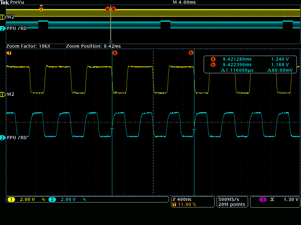 tek00061.png [ 31.92 KiB | Viewed 7130 times ]
Attachment:
File comment: Idle cycle
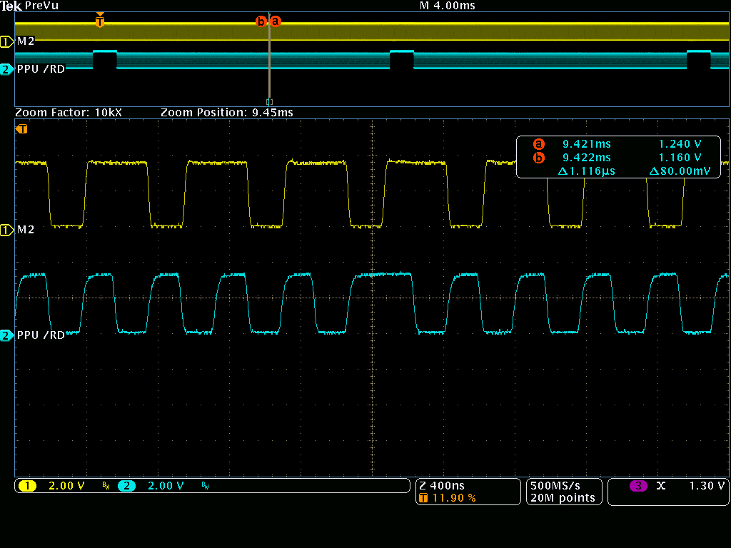 tek00062.png [ 30.37 KiB | Viewed 7130 times ]
Attachment:
File comment: Scope search function, pointing out all of the idle cycles
 tek00063.png [ 51.37 KiB | Viewed 7130 times ]
Edit:
I didn't look when I was using the scope but my calculations indicate that M2 and the PPU Idle cycle do not coincide in phase. In other words, the PPU Idle cycle will coincide with M2 Low (pictured), the first half of M2 high, or the last half of M2 high. So it cycles through the 3 phases each 3 scanlines. Not sure if that is important or not but it makes more sense why this state machine is so complicated. Will verify it with my scope tomorrow. For me, this stuff is the fun part.
Edit 2:
Confirmed that there is no way that the in-frame bit is setting and clearing for each scanline. That was 100% totally wrong, I screwed up. From what I am seeing now, my theory is that the scanline counter increments each time the bottom state machine becomes unlocked (which happens each scanline, only on PPU cycle 2), and the scanline counter resets each time that the top state machine becomes not-in-frame, which happens on scanline 240, cycle 6, 7, or 8, depending on M2/RD phase. Since there are 262 scanlines, which is not a multiple of 3, I do not believe that the M2/RD phase is the same from one frame to the next for scanline 240 (or any other particular scanline). Will need to verify these things.
Edit 3:
lidnariq wrote:
We've known the horizontal timing for more than a decade:
viewtopic.php?p=12379#p12379Drag wrote a test that took advantage of predictable peculiarities of the PPU's fetch sequence to clock the MMC5 IRQ an extra scanline:
viewtopic.php?f=9&t=7653I am going to hold off reading up on this stuff lidnariq and try to follow through to my own unbiased solutions first, then go back and compare to what you guys did over a decade ago. Hopefully there are differences! That would be exciting.
I was not completely right with the M2/RD phase, it acts in a way I don't quite understand yet when I look at the initial idle cycle of the pre-render frame in 3 sequential frames. In the 3 that I looked at, it had 2 different phases. Hmmmmmmmm... That would seem to suggest that not all frames are the exact same number of PPU cycles. I need to think about it more.
This stuff might not mean much but it has value to close the loop in my understanding so I can proceed correctly with MMC5 interacting with this.
Pictured is the idle cycle of the pre-render scanline for 3 sequential frames. I expected 1 of them to coincide with M2 low and it did not.
Attachment:
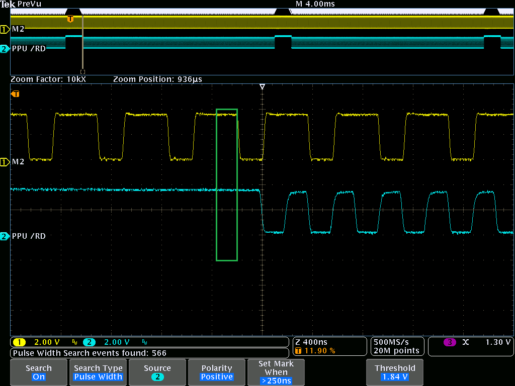 phase1.png [ 43.25 KiB | Viewed 7087 times ]
Attachment:
 phase2.png [ 43.32 KiB | Viewed 7087 times ]
Attachment:
 pahse3.png [ 42.79 KiB | Viewed 7087 times ]
Ben Boldt wrote:
I was not completely right with the M2/RD phase, it acts in a way I don't quite understand yet when I look at the initial idle cycle of the pre-render frame in 3 sequential frames. In the 3 that I looked at, it had 2 different phases. Hmmmmmmmm... That would seem to suggest that not all frames are the exact same number of PPU cycles. I need to think about it more.
Correct. We know the following two things:
1- The CPU and PPU use independent clock dividers, so the 2C02+2A03 have one of four different alignments randomly depending on power-up state
2- The 2C02 skips one pixel every other vblank when rendering is enabled. This makes the average frame length not 341*262 = 89342 pixels ( = 29780⅔ CPU cycles), but 89341.5 pixels (29780½ CPU cycles)
lidnariq wrote:
Ben Boldt wrote:
I was not completely right with the M2/RD phase, it acts in a way I don't quite understand yet when I look at the initial idle cycle of the pre-render frame in 3 sequential frames. In the 3 that I looked at, it had 2 different phases. Hmmmmmmmm... That would seem to suggest that not all frames are the exact same number of PPU cycles. I need to think about it more.
Correct. We know the following two things:
1- The CPU and PPU use independent clock dividers, so the 2C02+2A03 have one of four different alignments randomly depending on power-up state
2- The 2C02 skips one pixel every other vblank when rendering is enabled. This makes the average frame length not 341*262 = 89342 pixels ( = 29780⅔ CPU cycles), but 89341.5 pixels (29780½ CPU cycles)
Fascinating, do we know the purpose why it skips a cycle ever other v-blank like that?
To get a more desirable dot crawl pattern (cross-luma artifacts in composite video).
NewRisingSun wrote:
To get a more desirable dot crawl pattern (cross-luma artifacts in composite video).
Wow, I never cease to be amazed by this thing.
I wrote a test tonight that I expected to trigger the scanline IRQ on scanline #4. Interestingly, /IRQ stays always high for this test. Note that I tied all PPU address lines to GND and toggled PPU /A13 to select between PPU address $0000 and $2000. I verified that I have no M2 gaps larger than 10 usec.
Here is what this test does in english (numbers corresponding to the code below):
1. CPU Read from address $0000 11 times: 11 M2 toggles with PPU /RD = 1, to make it think not-in-frame
2. CPU Write $18 to $2001: Let the MMC5 sniff the PPU rendering being enabled, not likely necessary
10. CPU Read from $5204: Acknowledge any pending scanline IRQ
11. CPU write $04 to $5203: Set it to have an IRQ on scanline #4.
12. CPU write $80 to $5204: Enable the scanline IRQ.
20. While reading from PPU address $2000, read from CPU address $0000. (PPU read in range)
21. Repeat #20.
22. Repeat #20. 3 consecutive reads from PPU address $2000 have now occurred.
23. While reading from PPU address $0000, read from CPU address $0000. (PPU read out of range)
Loop back to step 20 300 times.
After 300 times, loop all the back to step 1.
I never get any /IRQ from this. Do you guys have any ideas what I should try? Unless I goofed up somewhere, it seems that this is not enough to trick the MMC5 to detect a scanline.
Code:
void writeOnCpuBus( uint16_t address, uint8_t data )
{
fast_m2_update( 0 ); // Set M2 low.
// Write CPU address bus:
OUTP_CPU_ADDRESS_BUS = (address ^ 0x7FFF);
// Write CPU data bus:
OUTP_CPU_DATA_BUS = data;
CPU_RW_PIN = 0; // MMC5 data bus as input
MACRO_SET_CPU_DATA_BUS_OUTPUT(); // Pic data bus as Output
asm(" repeat #12 \n\t nop "); // Setup Delay, so address and data busses are stable for MMC5 to register the write on M2 falling edge
fast_m2_update( 1 ); // M2 rising edge.
asm(" repeat #12 \n\t nop "); // Setup Delay, This delay improves expansion RAM writes big-time, not sure why.
fast_m2_update( 0 ); // M2 falling edge.
}
uint8_t readOnCpuBus( uint16_t address )
{
uint8_t result;
fast_m2_update( 0 );
MACRO_SET_CPU_DATA_BUS_INPUT(); // Pic data bus as Input
CPU_RW_PIN = 1; // MMC5 data bus as output
// Write CPU address bus:
OUTP_CPU_ADDRESS_BUS = (address ^ 0x7FFF);
asm(" repeat #12 \n\t nop "); // Setup Delay, so address bus is stable for MMC5 to register the read on M2 rising edge
fast_m2_update( 1 ); // Rising edge M2
asm(" repeat #12 \n\t nop "); // Setup Delay, for MMC5 to have data updated and stable on CPU address bus before reading it
result = (uint8_t)INP_CPU_DATA_BUS; // Capture CPU data bus
fast_m2_update( 0 ); // M2 falling edge.
return result;
}
void __attribute__((interrupt, no_auto_psv)) _T1Interrupt( void )
{
static uint16_t test_state = 0;
static uint16_t loop_count = 0;
static uint16_t lock = 0;
switch( test_state )
{
case 0: // Init
PPU_RD_PIN = 1;
loop_count = 0;
test_state++;
break;
case 1:
if( loop_count < 10 )
{
readOnCpuBus(0x0000);
loop_count++;
}
else
{
readOnCpuBus(0x0000);
test_state = 10;
loop_count = 0;
}
break;
case 10:
readOnCpuBus(0x5204); // Clear scanline IRQ
test_state++;
break;
case 11:
writeOnCpuBus(0x5203, 1); // Set scanline # on which to generate interrupt
test_state++;
break;
case 12:
writeOnCpuBus(0x5204, 0x80); // Enable scanline interrupt
PPU_A13_N = 0; // Set PPU address to $2000 (in range)
test_state = 20;//++;
break;
case 13:
readOnCpuBus(0x0000);
test_state = 20;
break;
case 20: // PPU read in range
PPU_RD_PIN = 0;
asm(" repeat #12 \n\t nop ");
readOnCpuBus(0x0000);
asm(" repeat #12 \n\t nop ");
PPU_RD_PIN = 1;
test_state++;
break;
case 21: // PPU read same
PPU_RD_PIN = 0;
asm(" repeat #12 \n\t nop ");
readOnCpuBus(0x0000);
asm(" repeat #12 \n\t nop ");
PPU_RD_PIN = 1;
test_state++;
break;
case 22: // PPU read same
PPU_RD_PIN = 0;
asm(" repeat #12 \n\t nop ");
readOnCpuBus(0x0000);
asm(" repeat #12 \n\t nop ");
PPU_RD_PIN = 1;
asm(" repeat #12 \n\t nop ");
PPU_A13_N = 1; // Set PPU address to $0000 (out of range)
test_state++;
break;
case 23: // PPU read out of range
PPU_RD_PIN = 0;
asm(" repeat #12 \n\t nop ");
readOnCpuBus(0x0000);
asm(" repeat #12 \n\t nop ");
PPU_RD_PIN = 1;
asm(" repeat #12 \n\t nop ");
PPU_A13_N = 0; // Set PPU address to $2000 (in range)
if( loop_count < 241 )
{
loop_count++;
test_state = 20;
}
else
{
readOnCpuBus(0x0000);
loop_count = 0;
test_state = 10;
}
break;
}
IFS0bits.T1IF = 0; // Clear Timer1 interrupt flag.
}
Edit:
It seems more like a setup or code issue now because when I add this step (MMC5A timer IRQ):
Code:
(case 2 changed to do test_state++)
case 3:
writeOnCpuBus(0x5209, 0x20); // Timer IRQ
test_state = 10;
break;
/IRQ still stays high.
Edit 2:
Verified that I can still read and write to the multiplier. This means the MMC5A is running and the CPU bus is fully functional. I ohmed out /IRQ back through to my breakout board, no problems. No positive or negative M2 pulses greater than 100 usec. I wonder why I can't get any IRQs?? I have never looked at /IRQ before now actually.
Edit 3:
I reverted my code and I DID get the timer /IRQ to work. So now I have a starting point to debug this. I think I'm pretty much snowed in at work tonight so I might have all sorts of time to kill working on this.
Edit 4:
Figured out my bug. I always forget, my CPU address bus gets inverted by my level shifters. In the read and write, I should have had:
OUTP_CPU_ADDRESS_BUS = (address ^ 0x7FFF);
This fixed it and I am now tricking the MMC5 to generate scanline interrupts. Will continue investigating and experimenting.
Edit 5:
Fascinating discovery. I noticed that my /IRQ was going back high momentarily in my 300 scanline loop. I blew that loop out to 5000 and captured with my scope. I find that the /IRQ automatically goes back high each 241 scanlines, and after that, triggers low again after the specified number of scanlines. I changed the value loaded into $5203, and the re-trigger of /IRQ followed the new value. In this loop, /IRQ goes high, goes low after x cycles ($5203) and then goes back high again, exactly 241 scanlines from the last time it went high.
Also, this proves that the value loaded into $5203 is preserved and not directly decremented as the wiki alludes to.
Edit 6:
It looks like the MMC5 generates an IRQ after detecting +2 from the number specified in $5203. For example, I set $5203 = $01 and the IRQ occurred on the 3rd scanline detected. Which means that it is not possible to trigger IRQ on the prerender scanline or on scanline 0.
When doing the 241-scanline auto-release of /IRQ, it retriggers exactly after the number specified by $5203, not +2. I am not sure what that means or if it is a realistic situation, but maybe it means something.
Attachment:
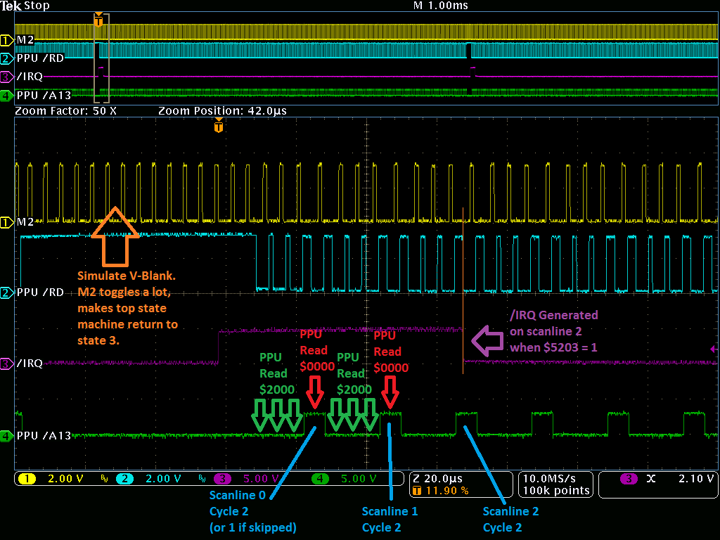 scanline_counter.png [ 60.55 KiB | Viewed 6913 times ]
Attachment:
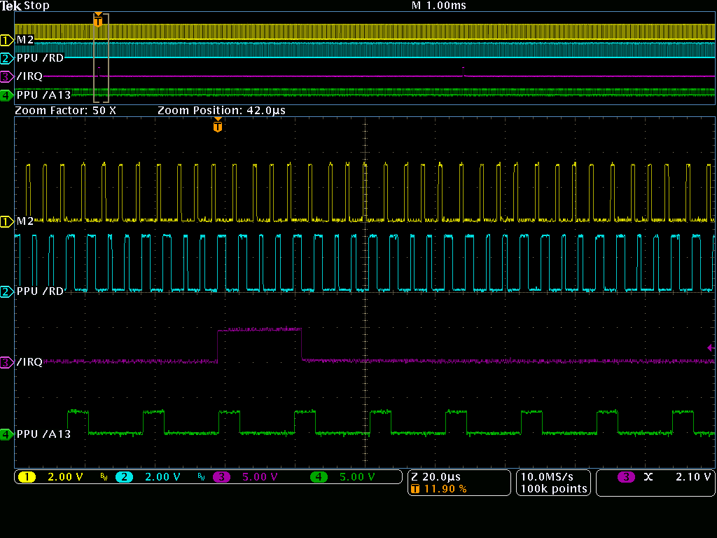 retrigger scanline.png [ 37.54 KiB | Viewed 6913 times ]
Edit 7:
I find that I do not have to write to $5203 again. It remembers the value. After I clear the /IRQ within the simulated v-blank, the IRQ occurs again on the correct scanline of the next frame.
Edit 8:
In the v-blank simulation period, where I had lots of M2 rising edges with PPU /RD high to get the top state machine into state 3, I reduced my M2 rising edges. When I went below 3, the 241-scanline rollover started kicking in, indicating that v-blank was no longer being detected by the MMC5. I now strongly believe that:
- Entering top state machine state 3 resets the scanline counter, i.e. in-frame status bit becomes 0.
- Entering the bottom state machine state 3 increments the scanline counter.
And it looks like this happens on PPU cycle 2 of each scanline (except for the pre-render scanline). This disagrees with the wiki, which states that the scanline IRQ occurs on cycle 0 of the scanline, and that the counter is incrementing somehow at the end of the previous scanline. Could we get into the details where this info came from? There should be a way to test and resolve the difference.
Edit 9:
Even if you simulate more than 241 scanlines between v-blanks, it is not possible to generate an IRQ when setting $5203 higher than 240, because that auto-release IRQ thing kicks in on the 241st scanline. I tried with 260 scanlines and $5203 = 241, /IRQ was always high. Also tried $5203 = 255, no difference.
Edit 10:
When I added a read from $FFFA within my simulated V-blank, then the IRQ occurs 1 scanline earlier. For example, if I set $5203 = 1, it will happen on cycle 2 of scanline 1.
Attachment:
File comment: With read of $FFFA within v-blank, scanline generating interrupt equals value written to $5203. $5203 = 1 shown here.
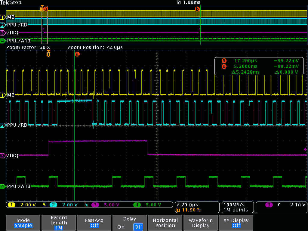 tek00076.png [ 49.93 KiB | Viewed 6910 times ]
Edit 11:
I think this is bad news for my beloved state machine diagram because I don't see how it captures edit 10. In my sumulated V-blank, I am not touching PPU/RD, and I have returned to already to state 3 (not-in-frame). By adding an additional read from $FFFA, it should make no difference according to this diagram -- the top state machine should stay in state 3 and the bottom state machine should remain unaffected.
This seems to suggest that the bottom state machine returns to unlocked state when reading $FFFA/B, which in itself increments the scanline counter, offsetting by this extra count observed. If this is true, it means that the next falling edge of /RD after reading $FFFA/B, regardless of any other condition or sequence, will set the "in frame" status bit back to 1. I am pretty sure that is not what we observed.
Edit 12:
False alarm. Whewww. It did not make any difference whether I read $FFFA/B. It always generates IRQ on the scanline in $5203 now. I am no longer able to recreate where it did the +1 I was seeing earlier, I am not quite sure what happened. I definitely changed too many things at once to keep track. I am updating the code above to the code I am using now.
Edit 13:
Shown here, I have $5203 set to 3. On the left I cause the MMC5 to reset the scanline counter via M2 rising edges with PPU /RD = 1. i.e., stepping through each state across the top state machine. On the right, I cause the MMC5 to reset the scanline counter by reading $FFFA. The behavior is shown to be the same in both cases, and consistent with the state diagrams.
Attachment:
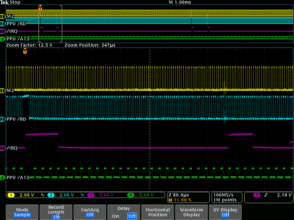 tek00077.png [ 51.08 KiB | Viewed 6909 times ]
Taking some time now to reflect on yesterday's experiments. Bottom state machine, going from unlocked to locked (i.e. state 3 to state 0), is what increments the scanline counter. Known fact from all of this, never found anything that disagrees with that.
This means that you read 3 consecutive matching PPU addresses in range $2xxx, followed by any number of additional PPU addresses, matching or not, in the range $2xxx. THEN any read outside the range $2xxx increments the scanline counter, in practice placing the IRQ actually on cycle 4 of the scanline. Simple enough, follows the diagram, we're happy.
However, I am not able to explain or reproduce the first screenshot in the previous post where it apparently did something else and was off by 1 extra scanline. I need to make it do that again somehow and try to explain it.
Another unknown: Does the top state machine reset the scanline counter when going from "in-frame" = 1 to 0, or from 0 to 1? It seems like 1 to 0 but was not investigated/confirmed.
One more note about the last screenshot, where I did both a simulated V-blank with 3 M2 rising edges with PPU /RD high, vs. reading from CPU $FFFA. I did not clear the interrupt in that test with the $FFFA. Reading it automatically cleared the IRQ back high on its own, similar to reading the 241st scanline. With this behavior, you could take a shortcut if you wanted to generate an IRQ on each N scanlines. For example, set $5203 = 8. Then when you are done in the scanline interrupt, simply read $FFFA and RTI. This will clear the IRQ, reset the scanline counter, and automatically generate another IRQ after 8 more scanlines.
Thanks to MPLabX's built-in history tracking, I was able to recover the old code that had an IRQ on the N+2 scanline. I did reproduce it.
Normally:
$5203 value -> IRQ happens in this scanline#, cycle #4
n/a -> Pre
n/a -> 0
1 -> 1
2 -> 2
3 -> 3
4 -> 4
And in this strange case:
$5203 value -> IRQ happens in this scanline#, cycle #4
n/a -> Pre
n/a -> 0
n/a -> 1
1 -> 2
2 -> 3
3 -> 4
I find that I can get into the strange case by changing the number of CPU reads in the simulated V-Blank with PPU /RD always high. Every multiple of 4 CPU reads inserted in this area causes the +1 offset to the scanline counter. This behavior is definitely not captured in the state diagrams. Neither state machine was previously believed to change any states when exceeding 3 consecutive M2 rising edges with PPU /RD always high. There is either something wrong with the diagram or there is another level of logic missing.
+1 on our understanding of MMC5 scanlines! Will try to narrow this and reconcile it with the status bit behavior.
Ben Boldt wrote:
by changing the number of CPU reads in the simulated V-Blank with PPU /RD always high. Every multiple of 4 CPU reads inserted in this area causes the +1 offset to the scanline counter.
O_o
Just to be clear: what exactly are you having /ROMSEL, M2, and R/W ... and I guess the whole address bus, really ... doing in this period?
lidnariq wrote:
Ben Boldt wrote:
by changing the number of CPU reads in the simulated V-Blank with PPU /RD always high. Every multiple of 4 CPU reads inserted in this area causes the +1 offset to the scanline counter.
O_o
Just to be clear: what exactly are you having /ROMSEL, M2, and R/W ... and I guess the whole address bus, really ... doing in this period?
This is all hooked directly to a dsPIC microcontroller, with no intervention from the PC. It has the source code loop I pasted above running directly on a hardware timer interrupt with nothing else going on. So it is very repeatable and no delays/lags/etc.
/ROMSEL and the CPU address bus are controlled directly by the PIC, all hooked up. M2, CPU R/W, PPU /RD, and PPU /A13 are also all direct to the PIC. PPU A0-A12 are all tied directly to GND.
When I change "if( loop_count < X )" in case 1 of the code, each 4th value X ends up with the +1 scanline behavior. I tried these values for X:
0 normal
1 normal
2 EXTRA
3 normal
4 normal
5 normal
6 EXTRA
7 normal
8 normal
9 normal
10 EXTRA
11 normal
12 normal
13 normal
14 EXTRA
15 normal
16
17
18 EXTRA
258 EXTRA
259 normal
65538 EXTRA (Note: in this case I changed to uint32_t type for loop_count.)
65539 normal
Maybe it cares how many M2s here in order to determine NTSC vs. PAL for some reason? Or maybe different PPUs have 2 prerender scanlines or something and it wants to skip an extra one? We only have 1 PPU timing diagram, for NTSC -- do we know the differences? Maybe that could shed some light.
Ben Boldt wrote:
OUTP_CPU_ADDRESS_BUS = (address ^ 0x7FFF);
In the NES, it's not /A15, it's literally NAND2(A15,M2). While I don't see how that would matter... I wouldn't dare rule it out.
Quote:
asm(" repeat #12 \n\t nop "); // Setup Delay, so address bus is stable for MMC5 to register the read on M2 rising edge
How fast is this dsPIC running? in other words, how many ns is 12 nops? Sorry for asking a question you may have already answered, but ... you kinda gave me a wall of text.
Quote:
void __attribute__((interrupt, no_auto_psv)) _T1Interrupt( void )
Step 2 in your synopsis is missing in your code, but I agree that it shouldn't matter.
What I'm really getting at is that the behavior you describe is incredible, because if a naive interpretation of what you say you observed were true, the MMC5 scanline IRQ would be unusable.
So I have to assume experimental error, but your notes are a sufficiently dense wall of text that I am having difficulty figuring out exactly what happened.
Quick things to test: Do other addresses other than 0 also cause the incorrect IRQ delay?
lidnariq wrote:
Ben Boldt wrote:
OUTP_CPU_ADDRESS_BUS = (address ^ 0x7FFF);
In the NES, it's not /A15, it's literally NAND2(A15,M2). While I don't see how that would matter... I wouldn't dare rule it out.
Okay, can change the test to behave this way.
lidnariq wrote:
Quote:
asm(" repeat #12 \n\t nop "); // Setup Delay, so address bus is stable for MMC5 to register the read on M2 rising edge
How fast is this dsPIC running? in other words, how many ns is 12 nops? Sorry for asking a question you may have already answered, but ... you kinda gave me a wall of text.
The dsPIC is running at ~40 MHz. I will measure the 12 nop delay for you.
lidnariq wrote:
Quote:
void __attribute__((interrupt, no_auto_psv)) _T1Interrupt( void )
Step 2 in your synopsis is missing in your code, but I agree that it shouldn't matter.
Yes, my bad. I had edited and updated the code but not the synopsis. You can consider the synopsis outdated in that post.
lidnariq wrote:
What I'm really getting at is that the behavior you describe is incredible, because if a naive interpretation of what you say you observed were true, the MMC5 scanline IRQ would be unusable.
So I have to assume experimental error, but your notes are a sufficiently dense wall of text that I am having difficulty figuring out exactly what happened.
Quick things to test: Do other addresses other than 0 also cause the incorrect IRQ delay?
Sorry I did put a lot of text up there, I wanted to capture every detail. I do these things after work before I go home, log it here, then I read it carefully on here at home at night so I can spend the time to think through it and plan what to try the next day. I had not taken the time to make my text more short and readable... Was getting hungry and went home.
I will try reading CPU addresses other than $0000 and let you know. Also, I will try doing a read of $FFFA at the beginning of the V-blank and see if that makes any difference. I am as confused as you are about this, it will be interesting to see where it goes. Hopefully it isn't some obscure issue with the way I have things set up, but really it is a pretty straightforward setup and code path. In case it's a real thing, let's continue to brainstorm why it might keep a count of M2 cycles and behave differently in 1 out of each 4 counts.
Isn't this awesome??? We have no idea how to explain this yet!
One potential issue is that my simulator is reading these addresses from PPU to simulate a new scanline:
$2000 (in range)
$2000 (matching)
$2000 (matching)
$0000 (not in range) <- IRQ observed here.
Whereas the real thing does this:
$2000 (in range)
$2000 (matching)
$2000 (matching)
$2xxx (AT read, in range, not matching)
$0000 (not in range) <- I think it should have IRQ here.
I will also check if this makes a difference to the extra scanline. I also plan to use a 74LS00 to make a bulletproof /ROMSEL signal.
I have modified my MMC5's PPU address bus setup today:
A0-9: All connected together to 1 digital output from microcontroller
A10-12: Always 0
/A13: Another digital output from microcontroller
This allows me to use these PPU addresses:
$0000 (Pattern table 0)
$2000 (Nametable 0)
$23FF (Attribute table 0)
and technically I could use PPU address $03FF (PT0), but no immediate use for that one. Will find some time this evening to try it.
Edit:
Additional hardware modification made today:
/ROMSEL used to be /A15. Now it is [A15 NAND M2] using a 74LS00 chip. This requires the code to send out A15 instead of /A15. Also, I put a toggle switch so I can change back easily.
We know that 3 PPU reads in a row from the same address are required to increment the scanline counter. We also know that the IRQ does not occur on the 3rd read, it has been observed on the 4th read.
My previous testing showed this:
1st read: in range $2xxx (tested $2000)
2nd read: matching 1st read (tested $2000)
3rd read: matching 1st read (tested $2000)
4th read: out of range. (tested $0000)
And the IRQ occurred on the 4th read. My testing today was to change the address of the 4th read. I replaced the 4th read with each of these addresses:
$0000
$2000
$23FF
All 3 of these addresses still caused the IRQ. Therefore, the 4th read does not care about the address matching, not matching, or in range. The IRQ then correlates to PPU cycle 4, confirming our previous understanding. Will make the appropriate adjustment to the wiki.
Edit:
New discovery: Can't detect scanline with 3 matching AT byte reads, i.e. 3 reads of $23FF in a row won't trigger scanline detection. It has to be in normal NT range. Will update wiki accordingly.
Edit :
I jumped the gun on that one. I had a setup issue with AT vs. NT, I had changed the $2xxx instead of the $x3FF part of the address. I will repeat this experiment more carefully later. When I made my change, I was no longer detecting scanlines, which was the basis that I thought the 3FF part mattered to the 3-in-a-row thing.
lidnariq wrote:
Quote:
asm(" repeat #12 \n\t nop "); // Setup Delay, so address bus is stable for MMC5 to register the read on M2 rising edge
How fast is this dsPIC running? in other words, how many ns is 12 nops?
My NOP delay is approx. 350nsec. M2 has a period of approx. 5 usec (200 kHz).
I have taken your feedback seriously and I am doing my best to review and reduce my text before posting. Also providing more pictures for clarity and to break things up.
In my test, I do 1 CPU read (i.e. M2 toggle) for every PPU read (i.e. PPU /RD toggle). On a real NES, I should be getting fewer M2 toggles with respect to PPU /RD toggles. This may be part of the explanation why I am able to have a skipped scanline when I have 4*N M2 toggles within my v-blank. Regardless if it is realistic or not, it may still prove to be insightful to internal operations of the MMC5. It is still 100% repeatable.
I tried a few experiments:
- Everything done with /ROMSEL = CPU_A15 NAND M2 now instead of just using /A15. No difference found.
- Triggering scanline detection this way: PPU read $2000, 2000, 2000, 23FF, 0000. Then loop that for each scanline. Can skip either 1, but not both, 23FF and 0000 for same behavior.
- Changing any particular one of the M2 toggles during V-blank to read from $FFFA instead of $0000 had no effect, as long as the overall number of M2 toggles remained the same.
- Same test, changing one of them to a write of $00 to register $2001, no effect, IRQ still generated, extra scanline at 4*N intact.
- I added a PPU read during one of the points in time that M2 was low during v-blank. This did change the offset of the 4*N. I had to add/subtract CPU reads after it to get back in sync with the 4*N again. Then if I bumped this PPU read up one spot (to occur after the next CPU read) then I had to add 1 additional CPU read after this to compensate and get the skipped scanline again.
Realistically, though, wouldn't the PPU's V-Blank have an identical number of M2 toggles each time? The extra/missing PPU idle cycle happens between the prerender scanline and scanline 0, so that might theoretically be ignored by this 4*N logic. To me, this kind of points back to NTSC vs. PAL detection, and skipping an extra scanline with PAL for example. Or maybe something having to do with the 4 different power-on states of M2 clock vs PPU clock? I am not really sure how this could be a setup problem anymore.
Scope shots:
Normal:
Attachment:
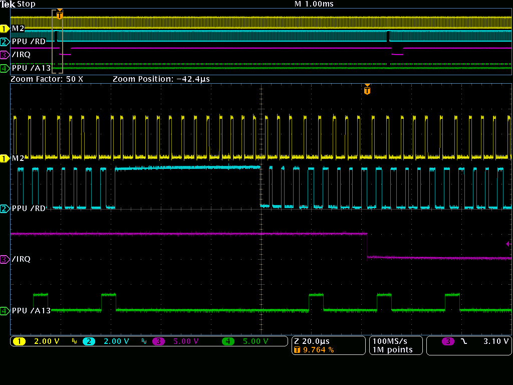 no_extra_scanline.png [ 45.32 KiB | Viewed 6401 times ]
Extra Scanline:
Attachment:
 extra_scanline.png [ 45.86 KiB | Viewed 6401 times ]
Next, I simulated full scanlines, instead of tricking the MMC5 with the least possible number of steps. A full scanline was simulated like this:
A. V-blank CPU $0000 reads, number of reads 4*N adjusted to find extra scanline.
B. PPU read $2000, 2000
C. PPU read $2000, 23FF, 0000, 0000.
D. Loop to C 42 times. (# of fetch sequences per scanline)
E. Loop to B 241 times. (# of scanlines)
F. Loop to A infinite times
Same behavior:
Was able to immediately detect scanline (3/4 M2s):
Attachment:
 tek00080.png [ 48.8 KiB | Viewed 6401 times ]
Could not immediately detect scanline (1/4 M2s):
Attachment:
 tek00081.png [ 48.06 KiB | Viewed 6401 times ]
If I skip step B for the pre-render scanline (like a real NES, i.e. scanline 260 does not end in the extra NT fetches), it
never misses a scanline.
Note: Edited text above.
Ben Boldt wrote:
Realistically, though, wouldn't the PPU's V-Blank have an identical number of M2 toggles each time?
Yes,
but I don't think the math follows? They also won't all be reads. We know that MMC5 works correctly on 2C02, 2C07 and I'm about 90% certain I've heard someone mention it work on the UA6538 also.
Vblank on 2C02 is (262-241)*341/3 = 2387cy ; ÷4 = 596 ; %241 = 114
Vblank on 2C07 is (312-241)*341/3.2 = 7565cy ; ÷4 = 1891 ; %241 = 204
Vblank on UA6538 is (312-241)*341/3 = 8070cy ; ÷4 = 2017 ; %241 = 89
so while it's conceivable that there's a special compensatory mechanism, it's far more likely that you're tickling undefined behavior.
Also, PPU/RD isn't doing anything during vblank, so it's not like there's any clock source for the MMC5 other than its internal 10µs timer and the CPU's 1.7-1.8MHz M2.
Quote:
no_extra_scanline.png
Oh, hm. Your test always asserts M2 only during a read. In practice, M2 is high for almost two pixels, so sometimes the two buses shouldn't align.
It does seem unlikely that that could be what's wrong, however.
Quote:
If I skip step B for the pre-render scanline (like a real NES, i.e. scanline 260 does not end in the extra NT fetches), it never misses a scanline.
So it looks like there's something being caught there that explicitly copies the scanline # over when the MMC5 detects the pre-render scanline, and you're getting some kind of uninitialized state here otherwise?
lidnariq wrote:
so while it's conceivable that there's a special compensatory mechanism, it's far more likely that you're tickling undefined behavior.
I agree with that completely.
The issue that we are seeing here is caused by a completely unnatural condition -- basically I have generated the 2 dummy nametable reads right before the prerender scanline, that are not normally there. Depending on the number of M2 toggles before these extra nametable reads, it may or may not trigger the scanline counter. Every 4th M2 toggle added does not trigger the scanline counter, the others do.
Our diagram explains the way that the in-frame status bit works. I believe strongly that there should be a way to converge the scanline counter's behavior with the status bit's behavior into 1 simple diagram, and ultimately into 1 accurate concise explanation.
Still not able to fit everything we know together in a simple/realistic way. I have a couple more tidbits from today.
I am able to take an additional shortcut getting the MMC5 to detect scanlines. If I do PPU reads always from address $2000, repeating, I get:
Read 1 (Matching 1)
Read 2 (Matching 2)
Read 3 (Matching 3)
Read 4 -> Scanline detected
Read 5 -> Another scanline detected
Read 6 -> Another scanline detected, etc.
Even with this shortcut, the first scanline is detected on Read 5 each 4*N number of M2s before Read 1.
Another note: I noticed on the "241st Scanline reset" thing, IRQ goes high on the RISING edge of PPU /RD. This my first observed action triggered from rising edge PPU /RD.
Attachment:
 tek00082.png [ 39.68 KiB | Viewed 6195 times ]
Something to consider: 'in frame' status bit might get set on scanline 0, however it is not ever possible to generate IRQ on scanline 0. There could be something lurking between scanline 0 detection and scanline 1
New discovery today.
Right when I enter the simulated V-Blank, I tried 1 additional PPU read, so I could easily control the address of the last PPU read before the series of M2 toggles. If the last PPU read was $2000, and then 3 M2 rising edges occur, it clears the IRQ, as we knew. But if I change the last PPU read to $23FF, $0000, or $03FF, it NEVER clears IRQ from M2. I tried 1000 toggles, /IRQ stayed low. I also made sure to try v-blanks with fewer than 241 scanlines between to make sure I wasn't conditionally triggering that function somehow. It made no difference.
This makes sense though -- the last thing the PPU does before V-blank is a dummy NT read from scanline 239, cycle 340. So the MMC5 sees this, then if there are 3 M2 rising edges in a row without any PPU reads, that is how it knows it is 'not in frame'. It doesn't explain the 1 in 4 thing we are seeing. One more piece of the puzzle though.
So ... that means we should be able to get wacky results on hardware if we turn of rendering using a mirror of the PPU's registers at exactly the right time?
lidnariq wrote:
So ... that means we should be able to get wacky results on hardware if we turn of rendering using a mirror of the PPU's registers at exactly the right time?
Concerning the MMC5 itself sniffing register $2001, I haven't actually seen any effect to the scanline counter when I do a write $00 to CPU address $2001. Is that what you are referring to? I have tried it and I do not believe it clears the scanline IRQ or resets the counter or anything like that.
I just did another experiment. With this 'last' PPU read before the M2 toggles. Before, I just left the PPU address bus intact with the address I was testing, so we didn't really know if it was latching the last PPU address on PPU/RD falling edge, or if it was still reading and using the address that's out there on the bus.
I tested by setting PPU address = $2000, PPU /RD low, then high, then changing PPU address to $0000 before proceeding to the M2 toggles. It still cleared the IRQ after the 3rd rising edge of M2 after this. SO, it does latch the fact that the last address was an NT byte, and not an AT byte or PT byte. It seems reasonable that it always keeps track of the entire previous PPU address for the purpose of finding matches anyway.
The in-frame flag doesn't directly affect IRQs?
lidnariq wrote:
The in-frame flag doesn't directly affect IRQs?
Are you saying that the in-frame flag clears when you write $00 to $2001? I think I missed that earlier - was that something krzysiobal found? I have not found $2001 to have any effect on scanline IRQ counting / setting / clearing so far but I should take another look.
It could be a 1-way street for scanline detection to trigger setting the in-frame flag but not the other way around.
I think krzysiobal found it also, but blargg mentioned something that looks awfully similar
a little while ago
lidnariq wrote:
I think krzysiobal found it also, but blargg mentioned something that looks awfully similar
a little while agoI guess 14 years isn't that long compared to the age of this system
Very interesting... I will have to devise a good way to read the status bit in this test and see what is going on. I am thinking about looking at CPU D6 and setting a pin of my micro during the read, then I can see it on the scope in real time. That should be cool and very helpful for further testing as well.
In this scope shot, marker A shows the last PPU read. Marker B shows where the 'in frame' status bit became zero. "Reading $5204" is a microcontroller pin I am setting when reading $5204. "In_frame" is CPU D6.
Because I am polling $5204 in order to read the status bit, it has acknowledged the IRQ, so we no longer see the IRQ auto-acknowledge in this situation. That was the function that depended on the last PPU address that was read.
Interestingly, the address of the last PPU read makes no difference in this situation. I set it to $2000, 23FF, 0000, and 03FF, and the status bit always went to 0 at the 3rd rising edge of M2. Note: PPU /A13 rises after the last read because I always set the PPU address bus back to $0000 after the last read now. i.e. /A13 high corresponds to $0xxx.
Attachment:
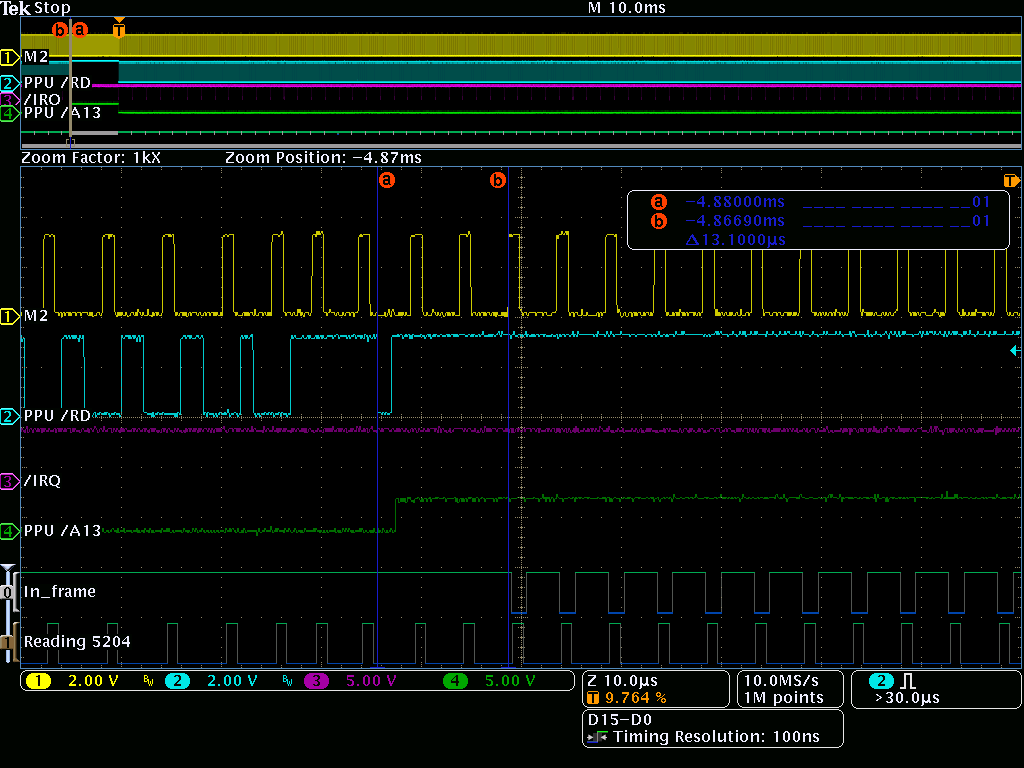 tek00083.png [ 38.81 KiB | Viewed 8478 times ]
So, since it takes four M2 from the write that disables rendering to the first time that the 2A03 can poll, it looks the same. But it appears that it's instead just timing out.
lidnariq wrote:
So, since it takes four M2 from the write that disables rendering to the first time that the 2A03 can poll, it looks the same. But it appears that it's instead just timing out.
I think so. I also tested adding write of $00 to $2001 at lots of different points in the sequence. At no point did it appear to have any effect at all to the status bit, the scanline IRQ, or the scanline counter. Again confirming what you are saying. I have clarified it in the wiki.
Behavior of 'in frame' bit at the beginning of each scanline (PPU cycle 4+) after V-Blank simulation, including unnaturally high numbers of scanlines:
Code:
Scanline detected -> Corresponding PPU scanline # -> 'in frame' status bit -> IRQ with $5203 = 1
1st -> Pre -> Not in Frame
2nd -> 0 -> In Frame
3rd -> 1 -> In Frame -> IRQ Triggered
4th -> 2 -> In Frame
[...]
240th -> 238 -> In Frame
241st -> 239 -> In Frame
242nd -> n/a -> Not in Frame
243rd -> n/a -> In Frame
244th -> n/a -> In Frame -> IRQ Triggered
245th -> n/a -> In Frame
[...]
482nd -> n/a -> In Frame
483rd -> n/a -> Not in Frame
484th -> n/a -> In frame
485th -> n/a -> In Frame -> IRQ Triggered
486th -> n/a -> In Frame
[...]
723rd -> n/a -> In Frame
724th -> n/a -> Not in Frame
725th -> n/a -> In frame
726th -> n/a -> In Frame -> IRQ Triggered
727th -> n/a -> In Frame
Bearing in mind that the pre-render scanline is not detected by the MMC5, because it is not preceded by the 2 dummy NT reads at the end of scanline 260, the 1st scanline doesn't really count. Showing math with '+1' below because of this.
This demonstrates/confirms that the scanline counter
resets at the 1 + 241st scanline, because it becomes 'not in frame' again at 1 + [241
* 2] = 483, and 1 + [241
* 3] = 724. And not for example, free-running an 8-bit counter that would roll over at 1 + [241
+ 256] = 498. The scanline IRQ also follows the counter reset and triggers again appropriately.
Showing 242nd scanline detected (as if PPU had visible scanline 240), then v-blank, then 1st scanline (PPU pre-render scanline):
Attachment:
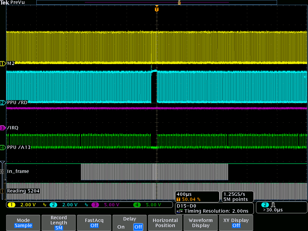 tek00084.png [ 52.02 KiB | Viewed 8397 times ]
EDIT:
Updated information above.
If an ExROM circuit board has a battery mounted, does that imply that EXRAM content is also retained, as is the case with the Namco 163 chip's internal RAM?
Quote:
If an ExROM circuit board has a battery mounted, does that imply that EXRAM content is also retained, as is the case with the Namco 163 chip's internal RAM?
Yes, this touched me with the Super Mario All Stars MMC5 where author used EXRAM to store a variable if the opening curtain has already been shown, causing it to show only one time after power-up or until batery was re-insterted.
On real hardware? So the answer is yes, EXRAM is preserved on battery-backed cartridges.
Oh, thank-you.
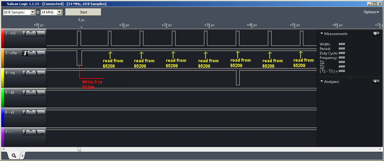

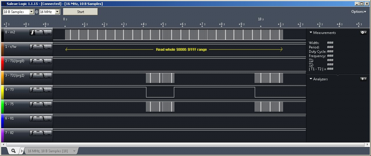

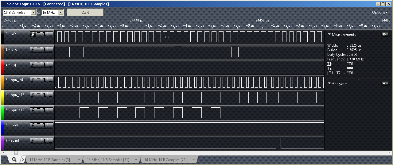


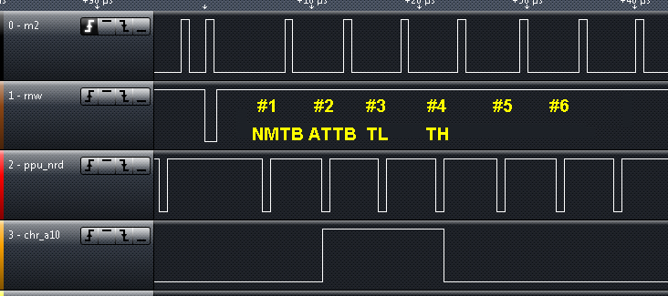
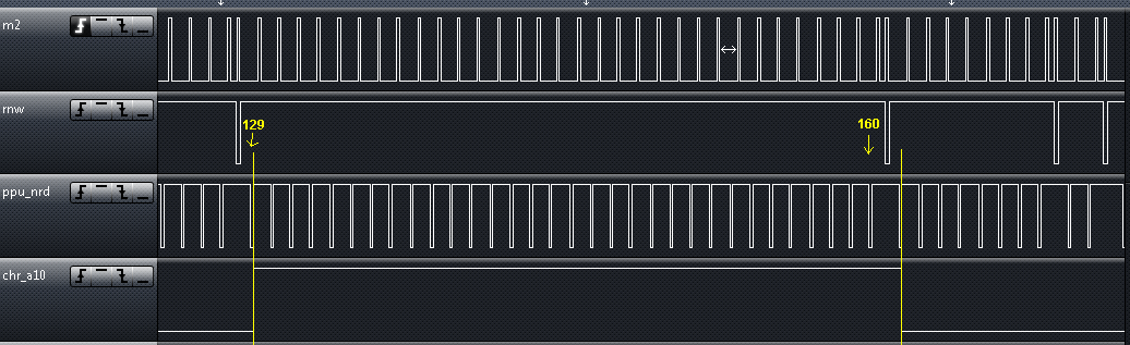