Hi, I bought the Kazzo cartridge "INL Retro" Dumper-Programmer to dump a 82 in 1 Chinese cart but I'm having trouble,
all the scripts I tested with Anago did not work, sorry for the lack of knowledge about it, it goes on Attach the photo of
the cartridge and the board. Thank you.
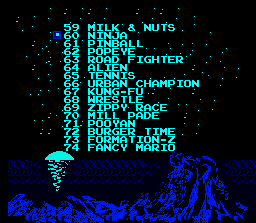
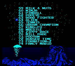
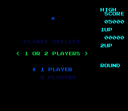
Game selection menu: ( youtube )
https://www.youtube.com/watch?v=uOhE7UNCNXk
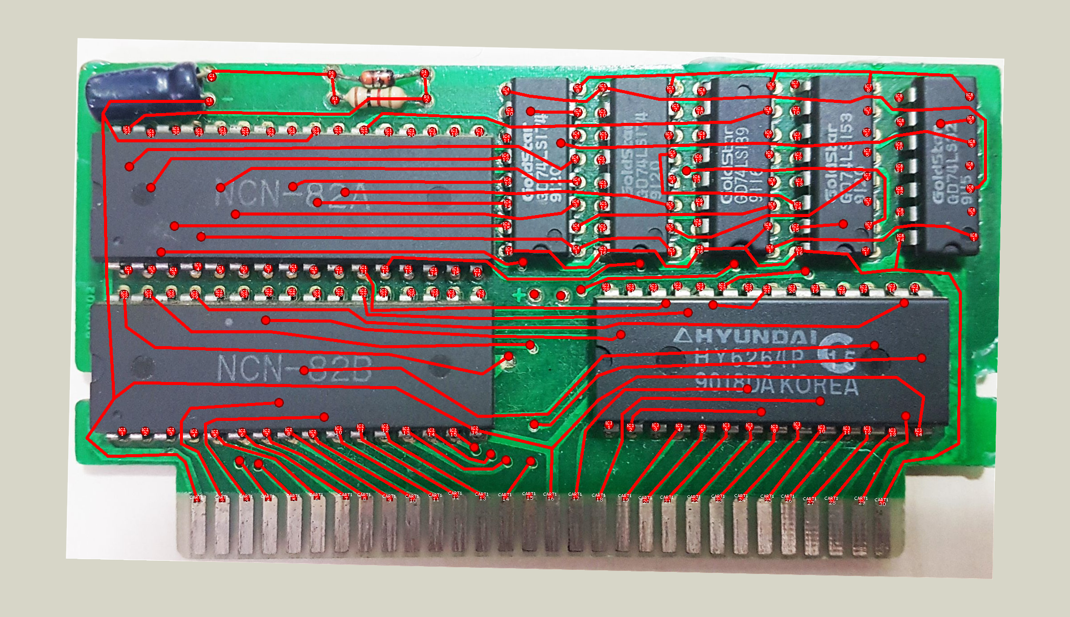
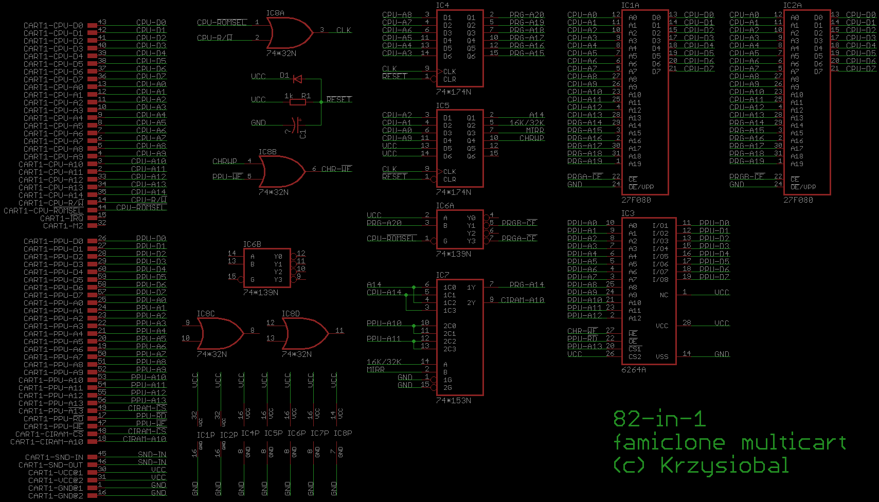
Cart Photos :
![IMG-20170815-WA0041[1].jpg](./download/file.php?id=9852&t=1)
IMG-20170815-WA0041[1].jpg [ 126.16 KiB | Viewed 2247 times ]
![IMG-20170815-WA0039[1].jpg](./download/file.php?id=9851&t=1)
IMG-20170815-WA0039[1].jpg [ 114.79 KiB | Viewed 2247 times ]
![IMG-20170815-WA0043[1].jpg](./download/file.php?id=9853&t=1)
IMG-20170815-WA0043[1].jpg [ 105.66 KiB | Viewed 2245 times ]
![IMG-20170815-WA0045[1].jpg](./download/file.php?id=9854&t=1)
IMG-20170815-WA0045[1].jpg [ 151.08 KiB | Viewed 2245 times ]
all the scripts I tested with Anago did not work, sorry for the lack of knowledge about it, it goes on Attach the photo of
the cartridge and the board. Thank you.
Game selection menu: ( youtube )
https://www.youtube.com/watch?v=uOhE7UNCNXk
Cart Photos :
Attachment:
IMG-20170815-WA0041[1].jpg [ 126.16 KiB | Viewed 2247 times ]
Attachment:
IMG-20170815-WA0039[1].jpg [ 114.79 KiB | Viewed 2247 times ]
Attachment:
IMG-20170815-WA0043[1].jpg [ 105.66 KiB | Viewed 2245 times ]
Attachment:
IMG-20170815-WA0045[1].jpg [ 151.08 KiB | Viewed 2245 times ]