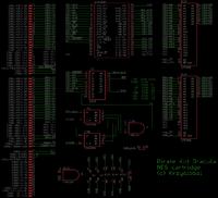
Hi.
This is the thread I promissed on the Kid Dracula (Akumajō Special: Boku Dracula-kun) reverse engineering.
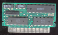
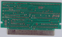
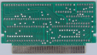
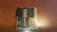
I'm posting the assembled card pictures first:
Attachment:
File comment: Kid Drac - Componentes
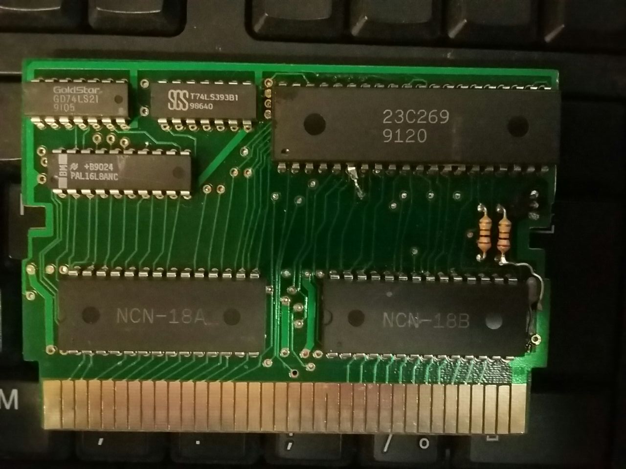 IMG-20161226-WA0006.jpg [ 136.51 KiB | Viewed 7913 times ]
Attachment:
File comment: Kid Drac - Solda
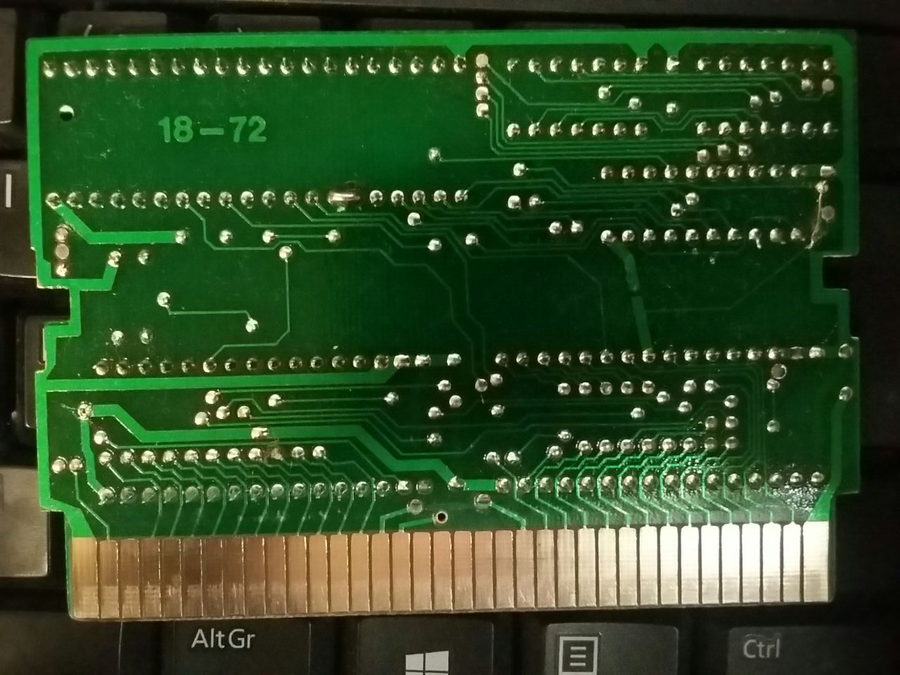 IMG-20161226-WA0007.jpg [ 163.82 KiB | Viewed 7913 times ]
I noticed some routing errors, there's possibly more:
1- Pins 6 and 7 of the 23c269 are swapped.
2- The CIC stun cicrcuit seems misrouted.
3- Pin 22 of the PRG? ROM is misrouted.
Next I'll post the naked board scans.
Get ready for some PCB porn!!
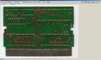
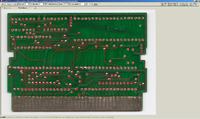
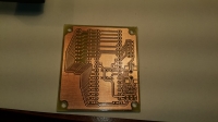
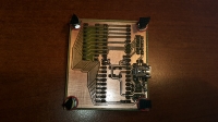
As promised, some PCB porn:
Attachment:
File comment: Kid Drac - Componentes
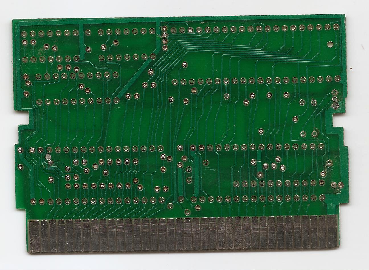 KidDrac - Componentes.png [ 1.66 MiB | Viewed 7912 times ]
Attachment:
File comment: Kid Drac - Solda
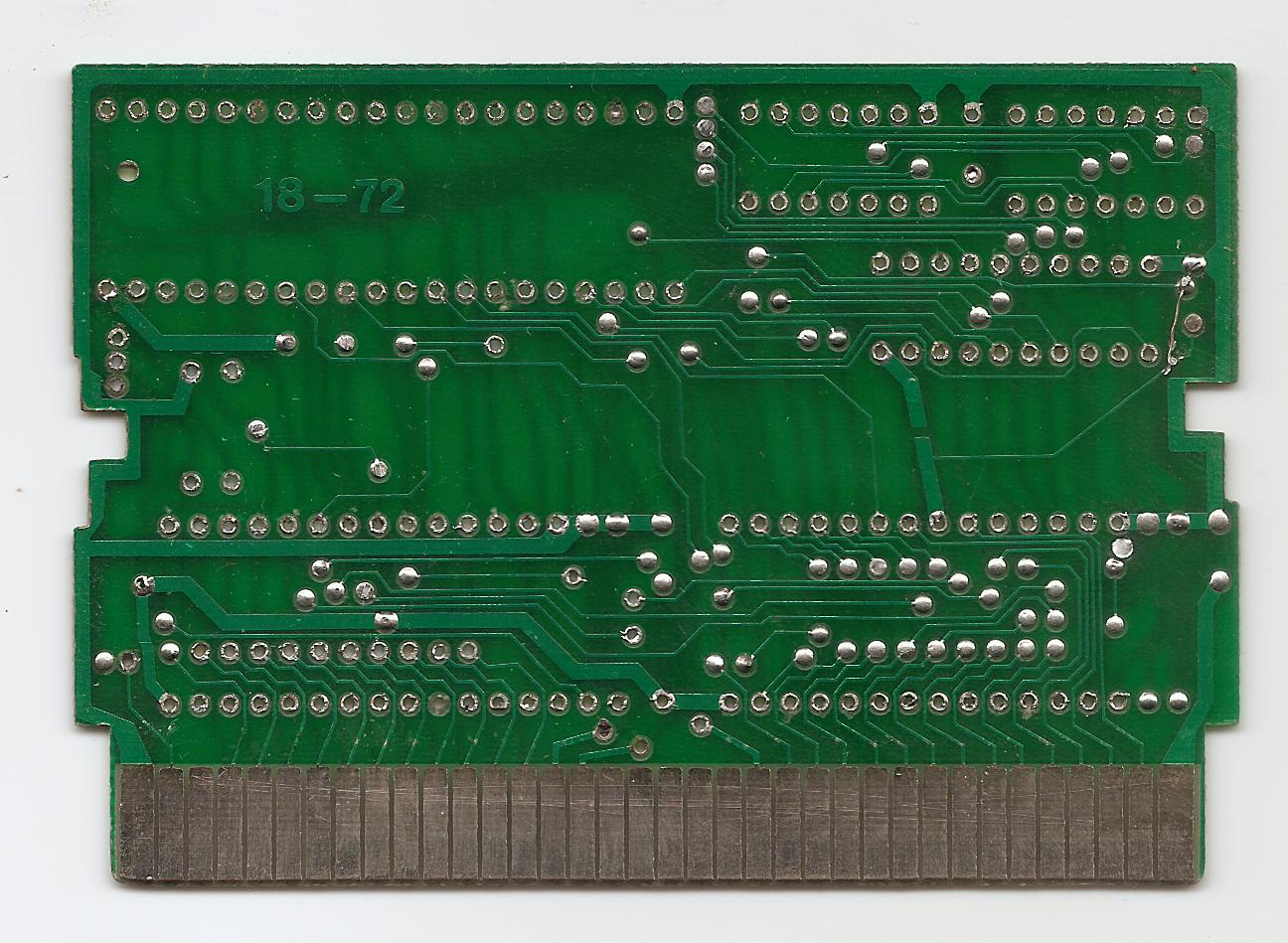 KidDrac - Solda.png [ 1.53 MiB | Viewed 7912 times ]
Next I plan to dump the PRG and CHR ROMs plus the PAL chip.
Can someone please tell me wich pins are inputs and wich are outputs on the PAL?
I'm with 9 guests at home (5 are kids) that will stay this whole week and part of the other, so it's better to do these dumps in a single shot!!
... This IRQ counts falling edges of PPU A13. Specifically, it counts 86 of them, or two scanlines.
Of the six pins that could be inputs or outputs, they are either all outputs or connected to nothing. They are probably all outputs.
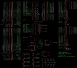
Tracing completed.
Fisher wrote:
I noticed some routing errors, there's possibly more:
1- Pibns 6 and 7 of the 23c269 are swapped.
2- The CIC stun cicrcuit seems misrouted.
3- Pin 22 of the PRG? ROM is misrouted.
This board is basically identical to the one zxbdragon took pictures of in
the other thread, modified to work in a NES instead of a Famicom (and use mask ROMs instead of EPROMs).
Pins 6 and 7 of the VRC2 clone are swapped because this board misroutes them. The NES swaps PPU A10 and A11 relative to the Famicom, and whoever modified this board for NES missed that key difference.
Pin 22 of a 28-pin mask ROM is A16, but the equivalent pin on EPROMs is /OE. You can see where both PRG and CHR had the trace connecting that pin to GND hastily cut, but only the CHR was correctly rerouted. The PRG was connected back to GND! The hack job connects it to the correct location.
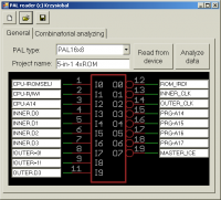
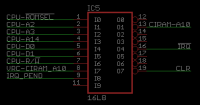
PAL pinout appears to be
Code:
.--V--.
/ROMSEL -> |1 20| -- +5V
CPU A2 -> |2 19| -> CNT CLEAR
CPU A3 -> |3 18| ?? nc
CPU A14 -> |4 17| ?? nc
CPU D0 -> |5 16| ?? nc
CPU D1 -> |6 15| ?? nc
R/W -> |7 14| -> /IRQ
VRC2 NTA10 -> |8 13| ?? nc
CNT=86 -> |9 12| -> CIRAM A10
Gnd -- |10 11| ?? nc
'-----'
But why not just use resistors as I suggested in the other thread?
thaks!Hope to be able to solve the MAPPER
Well Lidnariq, I really want to do that circuit, but my house is a little overpopulated...
Let me explain:
My sister is visiting me with her husband, she has 3 kids, plus, my niece is here with her husband too, and she has 2 other kids.
This makes me a
Uncle Grandpa!!I really fear that some kid come near me while I'm working and get hurt by any of the tools I have on my workdesk.
So it was kind of "Metal Gear" stealth action to hide myself and try to do at least part of the job.
Hope Everything was done correctly. You know: "haste makes waste"!
They really liked me and I have past most of my free time playing with them and my own kids.
Great job Krzysiobal!!
I just need to study and understand better these inner workings!!
I still consider myself a newbie in these stuff. Hope to change this soon!

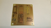
By the way, here is the PAL data I managed to dump:
Attachment:
File comment: Kid Drac PAL IC
 PALKIDDR.BIN [128 KiB]
Downloaded 311 times
The pinout I used:
Code:
.--V--.
A0 -> |1 20| -- +5
A1 -> |2 19| -> D5
A2 -> |3 18| -> D4
A3 -> |4 17| -> D3
A4 -> |5 16| ?? A10
A5 -> |6 15| -> D2
A6 -> |7 14| -> D6
A7 -> |8 13| -> D1
A8 -> |9 12| -> D0
Gnd -- |10 11| <- nc
'-----'
It's the same circuit I used to get that Gradius 2's PAL data, I only changed pin 14 to D6.
Hope this helps clarify even more how the IRQ circuit works.
If someone is interested, here is the ROMs dump,
I just don't know who is who.
Edit: Discovered who is who by comparing the CRC32 with Bootgod's site.
PRG ROM:
Edit: Removed to avoid future problems, as suggested.For reference:
NCN-18A.BIN CRC32 6a50b553
If someone needs it here's an IPS patch:
Attachment:
File comment: PRG ROM patch
 NCN-18A.ips [1.11 KiB]
Downloaded 305 times
Apply it to the original PRG ROM, CRC32 93794634
CHR ROM:
Edit: Removed to avoid future problems, as suggested.For reference:
NCN-18B.BIN CRC32 c5d1196e
The same CRC32 as the original.
If there's some problem posting this kind of stuff here, please, remove it.Edit: Removed possibly copyrighted material, as suggested.
Edit2: Fixed the NCN-18A.BIN, it was the same NCN-18B.BIN. Sorry...
Edit3: The CHR-ROM (NCN-18B.BIN) has the same CRC as the original.
Probably should delete the PRG and CHR dumps; unfortunately.
This exact dump is already in GoodNES 3.14 as "[p1][t1]"
(Interestingly, the PRG is also multiply present in multiple dumps, marked as "[b2]", "[p1][t1][b1]", and "[p1][t1]", and the CHR is "[!]", "[p1][t1]", "[t1]", and "[t2]")
Anyway, the PAL:
Pin 13 / D1 - does nothing at all, is always high.
Pin 15 / D2 - is low when writing to ((address & 0xC00C) == 0xC004) (edit, braino)
all other pins (12,17,18,19,14 = D0,3,4,5,6) are complicated, using feedback paths inside the PAL
So ... the PAL probably latches D0, D1 sometimes, and may count some number of overflows from the interrupt handler also. (Uh-oh)
Also, if you could re-dump with PAL pin 16 as an output that'd be nice.
lidnariq wrote:
Probably should delete the PRG and CHR dumps; unfortunately.
This exact dump is already in GoodNES 3.14 as "[p1][t1]"
(Interestingly, the PRG is also multiply present in multiple dumps, marked as "[b2]", "[p1][t1][b1]", and "[p1][t1]", and the CHR is "[!]", "[p1][t1]", "[t1]", and "[t2]")
Anyway, the PAL:
Pin 13 / D1 - does nothing at all, is always high.
Pin 15 / D2 - is low when writing to ((address & 0xC00C) == 0xC008)
all other pins (12,17,18,19,14 = D0,3,4,5,6) are complicated, using feedback paths inside the PAL
So ... the PAL probably latches D0, D1 sometimes, and may count some number of overflows from the interrupt handler also. (Uh-oh)
Also, if you could re-dump with PAL pin 16 as an output that'd be nice.
goodnes Sorting is imperfect.
[b] rom Many are GOOD DUMP,but is pirate.
After the game Kid Dracula IRQ emu.next MMC5 Clone PCb?
So, we know that the underlying VRC2 is VRC2b shaped. So all of the mapper accesses for CHR banking have to have been adjusted from the original game's VRC4e layout (0,4,8,C → 0,1,2,3).
There are up to eight possible registers in the PAL. The mask is $C00C.
The ones at $8000 and $C000 are explicitly no-ops to minimize how intrusive the patch had to be.
The one at $9004 (i.e. $8004) is the new augmented mirroring control register (since register mirroring will fall through to the VRC2 underneath). Two of the unknown five outputs on the PAL must latch D0 and D1 to keep track of when the PAL is supposed to override the mirroring.
There's one at $F004 (i.e. $C004); it doesn't pay attention to the data bus (the IRQ handler writes the contents of A as the very first thing). By context, this must restart the IRQ timer, keeping track of the number of times before it passes to the original IRQ handler.
The patch also writes to $9008, $F008, and $F00C; it's less immediately obvious what these are doing. After the nametable controls, and the idle bit, there are only two possibly volatile bits remaining. One is probably whether the IRQ is enabled... another may be whether the IRQ is currently asserted.
PAL pin 14 (dump D6) is 1 (IRQ not asserted) IF: /ROMSEL is 0 and CPUA2 is 1 and CPUA14 is 1 and R/W is 0. (i.e. $C004, $C00C)
— it's always 0 (IRQ asserted) IF: (pin 9) CNT=86, unless the immediate above line. More complicated behavior is hard to diagnose.
PAL pin 12 (dump D0) should, sometimes, be one of: pin 8 (A7) , logic 1, logic 0, depending. Additionally, it should be correlated with some other bits.
— Due to the in-order way the PAL-as-ROM was dumped, we can only tell that it does care about $8004 and does not care about writes to $8000, but write to $8008 or $800C cannot be determined.
PAL pin 17 and 18 (dump D3 and D4) appear to be the latched copy of CPUD1 and CPUD0 respectively in response to writes to the mirroring control register.
PAL pin 19 (dump D5) is asserted (i.e. reset counters) if: CNT=86.
—Otherwise, writes to $C008 seem to deassert it, and writes to $C00C seem to assert it
I'm not entirely certain what the next useful test would be. Maybe shuffling some address lines so that the dumper tickles things in a different order. Or maybe writing a test that could be put on some 'PROM to tickle the six different registers. And it would be really nice to massage the /ROMSEL input so that the PAL's latches-made-of-feedback-paths weren't glitchy...
He may well think of something... but here's what I'm confident of:
Code:
Mask: $C00C
$8000: no effect
$8004: [.... ..Mm] - mirroring override
||
|+-- 0: 1-screen A mirroring, 1: 1-screen B mirroring
+--- 0: Mirroring from VRC2, 1: Mirroring from m bit
These two bits are stored in the PAL's outputs-
M on pin 17
m on pin 18
$8008: Functionality not knowable from available dump
$800C: Functionality not knowable from available dump
$C000: no effect
$C004: Acknowledge IRQ
$C008: ?start IRQ counter?
$C00C: Acknowledge and ?stop counter?
Separately:
pin 12: (per pinout) Nametable override
pin 13: Nothing
pin 14: (per pinout) /IRQ
pin 15: IRQ ack
pin 16: not measured yet
pin 17: nametable override
pin 18: nametable 1screen override setting
pin 19: (per pinout) 74'393 +CLEAR
If one looks directly at the dump, each byte can be though of as a sequence of accesses to memory:
write "00" to $8000, idle, write to $8004, idle, write to $8008, idle … $800C $C000 $C004 $C008 $C00C, then the same for writing "01", "10", and "11"; then 64 cycles corresponding to reads from those same locations. Then 128 cycles while the nametable mirroring input is high instead of low.
Then 256 cycles while the 74'393 and 74'21 are indicating terminal count.
This pattern is repeated 256 times throughout the dump, showing a significant amount of variation is some outputs, hopefully due to violated timing constraints.
New PAL dump:
Attachment:
File comment: New PAL IC dump
 NEWPALKD.BIN [128 KiB]
Downloaded 305 times
Pinout used:
Code:
.--V--.
A0 -> |1 20| -- +5
A1 -> |2 19| -> D7
A2 -> |3 18| -> D6
A3 -> |4 17| -> D5
A4 -> |5 16| ?? D4
A5 -> |6 15| -> D3
A6 -> |7 14| -> D2
A7 -> |8 13| -> D1
A8 -> |9 12| -> D0
Gnd -- |10 11| <- nc
'-----'
I'm planning to do another dump later, using interleaved address lines (A0, A2, A4, A6, A8, A10, A12 and A14).
Would this be usefull?
Hm. I don't think skipping address lines would be helpful. I tentatively think reversing them should?
That would change the virtual bus behavior to instead look like
Write '00' to $8000 while not terminal count and input nametable=0
Write '00' to $8000 while terminal count and input nametable=0
repeat above, but input nametable=1
repeat above, but reading from $8000 instead
repeat above, but data bus now holds '10', then '01', then '11'
repeat above, but to $C000, then $8008, then $C008, then $8004, then $C004, then $800C, then $C00C
finally 65536 samples while /ROMSEL is high, which if my mental model is right, ought to ignore every pin other than pin 9/A8/"terminal count"
Because the 16L8 has six feedback loops, instead of registers, that means it has to be storing values in a multiplexer-like behavior, rather than caring about edges. So hopefully keeping things like this will help...
Another option could be to write a MS-DOS program that do any tests needed, assuming the PAL IC is present in the place of the BIOS ROM.
How difficult would this be?
For me, unfortunatelly, it's almost impossible

I mean, it wouldn't be hard to build an ISA card and some software to let you try exploring what's going on.
But I doubt it would be more useful than just writing a simple NES test ROM to see what happens in a reassembled cart, replacing the existing PRG.
The VRC2 should even have a single bit of tristate-able buffer (from pin 16 to CPU D0 during reads from $6000-$6FFF) that would let us test any single output from the PAL at a time, as long as it holds state (i.e. is slow). Assuming that this pirate clone bothered to copy that part... If it doesn't work, we could still add external parts to read any latched state instead.
PRG,CHR address is VRC2
IRQ address
FF00 : not using?
FF04 : counter?
FF08 : enabled?
FF0C : disabled?
clock?
Per the mapper hack's code, $FF04 has to be "acknowledge IRQ, do not stop", because that's how the game implements a variable number of scanlines IRQ (It uses the byte of RAM at $07F8 to count down some number of two-scanlines)
lidnariq wrote:
Per the mapper hack's code, $FF04 has to be "acknowledge IRQ, do not stop", because that's how the game implements a variable number of scanlines IRQ (It uses the byte of RAM at $07F8 to count down some number of two-scanlines)
yes,I know 0x07F8,but same pcb TNMT J. not using 0x7F8
Are we violently agreeing and just having problems due to lack of fluency in a common language?
lidnariq wrote:
Are we violently agreeing and just having problems due to lack of fluency in a common language?
......
lidnariq wrote:
Code:
$C004: Acknowledge IRQ
$C008: ?start IRQ counter?
$C00C: Acknowledge and ?stop counter?
It looks like $C004 and $C00C both acknowledge the IRQ, and $C00C additionally resets the counter. I don't see anything that looks like it would stop the counter, but I'm not sure about preventing IRQs.
lidnariq wrote:
pin 16: not measured yet
According to the newer dump, this looks like (inverted) writes to $C00C, but it's inconsistent in some places.
lidnariq wrote:
showing a significant amount of variation is some outputs, hopefully due to violated timing constraints.
That might be fixed by using a /CE or /OE signal on pin 1, if there happens to be one available, instead of an address line.
Well, I asked about the MS-DOS program because my dumper is just an old motherboard repurposed.
To be more precise, it's a
M748LMR, on wich I have soldered a 20 pin socket at bios' side and use UniFlash to dump.
But I sure can socket a PRG ROM on the cartridge board and do any tests needed.
My next step is to invert the adress pins and dump the PAL IC again.
It'll just take a litle more time than I want.
Joe, I think I can do a fast redump by pulling pin 1 low or high, or even plugging it to /CE or /OE.
What would help more?
Fisher wrote:
Well, I asked about the MS-DOS program because my dumper is just an old motherboard repurposed.
It'd be faster for you to just scramble the address lines you're using and dump it again. Lidnariq could probably tell you which combination(s) would be the most useful. It may also help if you could invert the signals on PAL pin 2 and/or pin 3.
Fisher wrote:
But I sure can socket a PRG ROM on the cartridge board and do any tests needed.
I won't be writing test ROMs any time soon. Maybe lidnariq will.
Fisher wrote:
Joe, I think I can do a fast redump by pulling pin 1 low or high, or even plugging it to /CE or /OE.
What would help more?
I suspect /OE will be more useful than /CE, but we won't know until you try. Pulling it low or high won't tell us anything useful.
The PAL uses pin 1 to detect when the values on pins 2 through 7 are valid. On the NES, /ROMSEL is only low when the other signals are valid. On your motherboard, A0 makes no such guarantee, but hopefully /OE or /CE will.
... right, if you're using a motherboard to dump the PALs, that explains the glitchy behavior, because the address bus probably isn't idle between fetches...
As far as useful orders: I think the most helpful minimal change would be to try all the combinations of D0, D1 before the address lines, by moving pins 2-4 to instead connect to dumper A9-A11, rather than doing a full reversing of pins.
Ok, I'm really tired... Played with the kids on the park almost all afternoon.
Let's see if I understand: Ineed to solder pins 2, 3 and 4 to A9, A10 and A11. Is it correct?
I plan to do it tomorrow, probably at work. (yes, I'll procrastinate!!)
Quote:
Let's see if I understand: I need to solder pins 2, 3 and 4 to A9, A10 and A11. Is it correct?
That's the easiest thing I can think of that should produce useful results.
I'm only confident that that will provide the information necessary to figure out whether $8008 and $800C do anything. Hopefully it'll demonstrate what's going on with $C008 and $C00C too, but I'm not certain about that yet.
Unrelatedly, I was looking more closely at the PAL16L8 datasheet, and noticed that pins 19 and 12 are
always outputs, and can
never be used as feedback terms inside. So they have to exclusively be a function of the other pins, which makes them really convenient for logic function reduction.
Apparently:
Pin 19 (counter clear) is 1 iff Pin 8 (Cnt=86) is 1 OR pin 16 is 0
Pin 12 (CIRAMA10) is: if Pin 17 ($9004q1 is 1) then Pin 18 ($9004q0) else Pin 7 (VRC2Mirroring)
And it turns out two more pins don't involve any feedback loops ... but we already knew these:
Pin 13 is 1
Pin 15 is 1 iff A2 is 0, or A14 is 0, or R/W is 1, or /ROMSEL is 1 → detects writes to $F004 and $F00C
The other four pins (pin 14 /IRQ, pin 17 $8004q0, pin 18 $8004q1, pin16) involve feedback loops, how inconvenient.
Pin 16 is definitely always 1 during writes to $C008. It is definitely always 0 during writes to $C00C .. but interestingly, it looks like it doesn't care about /ROMSEL?
If I look at the combination of pins 14, 15, 16, and 19, only eight of the sixteen possibilities ever exist, the following never occur:
Pins 19(CLR) and 16 both clear (duh, per above)
Pins 14(/IRQ) and 15 both clear (hmm)
all four pins high (hmm?)
I'll think about this some more and see if anything comes to mind re: pin 14 and 16.
Ok, I made 3 dumps:
1- Pin 1 on /CE:
Attachment:
File comment: Pin 1 on /CE
 PALKDCE.BIN [128 KiB]
Downloaded 152 times
2- Pin 1 on /OE:
Attachment:
File comment: Pin 1 on /OE
 PALKDOE.BIN [128 KiB]
Downloaded 153 times
3- Lidnariq's request:
Attachment:
File comment: Lidnariq's request
 PALDKLID.BIN [128 KiB]
Downloaded 154 times
Pin2 --> A9
Pin3 --> A10
Pin4 --> A11
The pinout is the same as I posted before, except for the pins I told I switched.
If there's anything else I can do just tell me and I'll make as fast as I can.
Ok, the dump for me that tells me that writes to $8008 and $800C are no-ops also.
The dumps for Joe where socket /CE is connected to PAL pin 1=/ROMSEL does also illuminate a few things... It really looks like D4=pin16 keeps track of which of $C008 (storing 1) and $C00C (storing 0) was most recently written to. Which ... would combine with D7=pin19 to mean that, yes, $C008 is "start counter", and $C00C is "ack IRQ and hold counter at 0"
I guess I could write a simple real mode program on your DOS machine... what program are you currently using to dump things?
... but I kinda feel like I've got a complete mental model of what's happening now, so maybe there's no need?
I'm dumping using Uniflash and a compact flash in a IDE adaptor.
The CF makes easy to upload stuff.
I can do anything that's necessary to RE this.
It can be faster if I don't need to modify the hardware.
If I remember correctly, Uniflash's source was released sometime ago.
It is written in Pascal, if I remember well.
Maybe this can be useful. Can it?
Hm, I found it:
http://www.rainbow-software.org/uniflash/but I never learned Pascal and don't yet have a copy of Turbo Pascal on hand...
Let's see if I can summarize what things I believe are true with the new data:
* Pins 12, 13, 15, 19 are
known exactly* Pins 17 and 18 are "latched value of D1 and D0 on writes to $8004"
* Pin 16 seems to be "become high on write to $C008; become low on write to $C00C; otherwise retain state"
* Pin 14 (/IRQ) seems to be "become high on write to $C004 or $C00C; become low when ((Cnt&86)==86); otherwise retain state"
So I think we can describe exactly what's going on now?
Mask: $C00C
- Writes to $8000, $8008, $800C, $C000: ignored
- Writes to $8004:
same as last time- Writes to $C004: Acknowledge IRQ
- Writes to $C008: Allow counter to run
- Writes to $C00C: Acknowledge IRQ and hold counter at 0
Counter counts PPU A13
falling edges; after 86 (two scanlines) it automatically zeroes its counter and asserts /IRQ.
This style of IRQ means that the program could explicitly choose an X coordinate (within 8 pixel granularity) where to get IRQs by clocking it a few times in vblank (
ldx #$FF / stx $2006 / stx $2006 / bit $2007) before rendering starts. There should be no X drift due to IRQ latency.
Does this sound right to the other people looking?
Great guys!!
Seems to be almost finished.
Just let me know when I can put this thing back together (when no more tests/dumps are needed).
I hope that zxbdragon finally can fgure out the inner workings of this pirate cartridge.
It's really nice to help.
Thank you!But I have no solve this IRQ.I'll wait for JOE!
zxbdragon wrote:
I'll wait for JOE!
I'll take a look on Monday and write the mapper doc if we've got everything figured out. (I'm on vacation this weekend.)
I didn't see anything that disagreed with lidnariq, so here's the mapper doc in Disch's style.
Code:
========================
= Mapper "18-72" =
========================
Example Games:
--------------------------
Akumajou Special: Boku Dracula-kun (pirate version)
Notes:
--------------------------
This mapper is another pirate VRC2b, this time with IRQs and VRC4-style
mirroring.
A mapper number hasn't been assigned to this particular board yet.
Registers:
---------------------------
There are two sets of registers: the VRC2 registers, and the Extra registers.
Writes will affect both sets of registers!
VRC2 registers range, mask: $8000-$FFFF, $F003
$8000-$8003: [...P PPPP] Same as VRC2b (PRG select 0)
$9000-$9003: [.... ...M] VRC2 mirroring control (see extra registers)
|
+- 0: vertical (A10); 1: horizontal (A11)
$A000-$A003: [...P PPPP] Same as VRC2b (PRG select 1)
$B000-$E003: [.... CCCC] Same as VRC2b (CHR select)
Extra registers range, mask: $8000-$FFFF, $C00C
$8004: [.... ..XX] Extended mirroring control
||
++- Extended mirroring control
0x: Let VRC2 control mirroring
10: one-screen, lower bank (overrides VRC2)
11: one-screen, upper bank (overrides VRC2)
$C004: [.... ....] Acknowledge IRQ
$C008: [.... ....] Start IRQ counter
$C00C: [.... ....] Acknowledge IRQ and hold IRQ counter at 0
Mirroring behavior:
---------------------------
Games will write to $9004 to affect both the VRC2 mirroring register ($9000)
and the Extra mirroring register ($8004) at the same time. The result is like
VRC4 mirroring:
$9004 [.... ..MM] Combined VRC2 and Extra mirroring control
||
++- VRC4 mirroring
00: Vertical
01: Horizontal
10: One-screen, lower bank
11: One-screen, upper bank
The VRC2 will remember the last setting written to it, even if the Extra
mirroring control is overriding it.
IRQ behavior:
---------------------------
The IRQ counter counts falling edges of PPU A13. The IRQ is asserted every time
the counter reaches 86. When the counter reaches 86, it's automatically reset
to 0. This results in one IRQ every two scanlines, as long as the counter is
running. Writing to Extra register $C004 or $C00C will acknowledge the IRQ.
Writing to Extra register $C00C will hold the counter at 0, and writing to
Extra register $C008 will allow the counter to resume.
Games will typically write to addresses like $F004/$F008/$F00C to control the
IRQ without affecting the VRC2's registers.
Let me know if you have any questions or spot any mistakes.
Joe wrote:
I didn't see anything that disagreed with lidnariq, so here's the mapper doc in Disch's style.
Code:
========================
= Mapper "18-72" =
========================
Example Games:
--------------------------
Akumajou Special: Boku Dracula-kun (pirate version)
Notes:
--------------------------
This mapper is another pirate VRC2b, this time with IRQs and VRC4-style
mirroring.
A mapper number hasn't been assigned to this particular board yet.
Registers:
---------------------------
There are two sets of registers: the VRC2 registers, and the Extra registers.
Writes will affect both sets of registers!
VRC2 registers range, mask: $8000-$FFFF, $F003
$8000-$8003: [...P PPPP] Same as VRC2b (PRG select 0)
$9000-$9003: [.... ...M] VRC2 mirroring control (see extra registers)
|
+- 0: vertical (A10); 1: horizontal (A11)
$A000-$A003: [...P PPPP] Same as VRC2b (PRG select 1)
$B000-$E003: [.... CCCC] Same as VRC2b (CHR select)
Extra registers range, mask: $8000-$FFFF, $C00C
$8004: [.... ..XX] Extended mirroring control
||
++- Extended mirroring control
0x: Let VRC2 control mirroring
10: one-screen, lower bank (overrides VRC2)
11: one-screen, upper bank (overrides VRC2)
$C004: [.... ....] Acknowledge IRQ
$C008: [.... ....] Start IRQ counter
$C00C: [.... ....] Acknowledge IRQ and hold IRQ counter at 0
Mirroring behavior:
---------------------------
Games will write to $9004 to affect both the VRC2 mirroring register ($9000)
and the Extra mirroring register ($8004) at the same time. The result is like
VRC4 mirroring:
$9004 [.... ..MM] Combined VRC2 and Extra mirroring control
||
++- VRC4 mirroring
00: Vertical
01: Horizontal
10: One-screen, lower bank
11: One-screen, upper bank
The VRC2 will remember the last setting written to it, even if the Extra
mirroring control is overriding it.
IRQ behavior:
---------------------------
The IRQ counter counts falling edges of PPU A13. The IRQ is asserted every time
the counter reaches 86. When the counter reaches 86, it's automatically reset
to 0. This results in one IRQ every two scanlines, as long as the counter is
running. Writing to Extra register $C004 or $C00C will acknowledge the IRQ.
Writing to Extra register $C00C will hold the counter at 0, and writing to
Extra register $C008 will allow the counter to resume.
Games will typically write to addresses like $F004/$F008/$F00C to control the
IRQ without affecting the VRC2's registers.
Let me know if you have any questions or spot any mistakes.
Thank you! I to try.
It's better if have FCEUX code
Try to fail
c008
counter = data?
clock
is
counter++;
if(counter >=86)
{
counter=0;
return true;
}
?
zxbdragon wrote:
c008
counter = data?
No—there's no way for the data to get into the counter
Quote:
counter++;
if(counter >=86)
{
counter=0;
return true;
}?
That does look like what I think FCEUX IRQs do. How are you getting a callback on every falling edge of PPU A13?
If there's no way for that, you
might be able to fake this with a normal FCEUX IRQ that fires every other scanline, but I don't know if that'll work.
Joe wrote:
Mapper "18-72"
I might tentatively use the label on the mask ROMs, "NCN-18"
lidnariq wrote:
zxbdragon wrote:
c008
counter = data?
No—there's no way for the data to get into the counter
Quote:
counter++;
if(counter >=86)
{
counter=0;
return true;
}?
That does look like what I think FCEUX IRQs do. How are you getting a callback on every falling edge of PPU A13?
If there's no way for that, you
might be able to fake this with a normal FCEUX IRQ that fires every other scanline, but I don't know if that'll work.
Joe wrote:
Mapper "18-72"
I might tentatively use the label on the mask ROMs, "NCN-18"
I can't solve
Yeah, I suspect that FCEUX doesn't give you the tools necessary to implement this mapper.
Well, looks like the hardware was all figured out.
I think my small paricipation is over.
Should I reassemble the cartridge?
I think we're set, and you should feel free.
Cool.
I'm really glad I could help.
It looks like Nestopia, also, only supports M2- and PPUA12- based IRQs. I have no idea if any existing emulator can support this mapper hack authentically.
Hey, looks like it's emulation is troublesome!!
Just a small epilogue... when I bought it, the vendor
sold me cheaper because it was "defective":
Attachment:
File comment: KidDrac defect
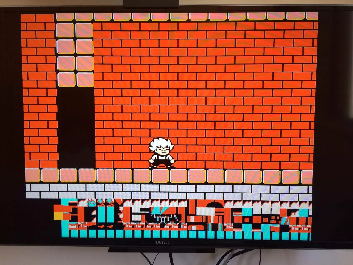 dracula-kid-nes-72-pinos-pi-D_NQ_NP_449405-MLB25022752776_082016-F.png [ 1.16 MiB | Viewed 4251 times ]
I took the risk and bought it anyway, since it was playable at least.
I tested it in a couple of clones and this supposed deffect never showd up.
Looks like the defect was on his console, who knows...
joe,can you working fine?
Fisher wrote:
So it was kind of "Metal Gear" stealth action to hide myself and try to do at least part of the job.
I think that it's more of a Splinter Cell scenario in your case,
Fisher.sorry
zxbdragon wrote:
joe,can you working fine?
Is there an emulator that can use PPU A13 to generate IRQs? (MMC3 uses PPU A12 to generate IRQs.)
Otherwise, you can use a hack to generate one IRQ for every two scanlines (count += 43 on each scanline), but timing won't be correct.
Quote:
I think that it's more of a Splinter Cell scenario in your case, Fisher.
Oh yeah!

People keep saying I should play that series of games, and I always keep forgotting.

Code:
sorry
Don't feel sorry!
It was a joke, intended to someone else to laugh and joke too, like you did.

Joe and Zxbdragon, I think proper support for this pirate mapper would need a rewrite of the emulator's core. Would it?
For a user's perspective this would not do much difference, since the original game is already playable.
But the on the developer's side, it's the challenge of doing it properly that makes all the difference.
If I'm understanding properly what I've been reading, this is the fuel that keeps emulation community as a whole active.
So I say: Power to you guys! Don't give up.
As a old boss I had said: The impossible is only a little bit protracted. (hope I have translated it right)
Fisher wrote:
Joe and Zxbdragon, I think proper support for this pirate mapper would need a rewrite of the emulator's core. Would it?
That depends on the emulator. I've only looked at FCEUX, and it doesn't provide any way for the mapper to track PPU A13. The easy hack would be to just trigger the IRQ every other scanline, but timing would be wrong. It may be possible to do it better using a combination of scanline and CPU-cycle counters in FCEUX, but that's more work than I'm willing to put into this (and probably still wouldn't be accurate).
If there's an emulator core that has some way for the mapper to track the PPU A13 line, then I'll give it a shot.
Nestopia's code base also seems to have only implemented support for PPU A12 and M2-based IRQs, even though the OO goo makes it look like it should be more useful... ("What do you mean no one ever implemented Nst::Core::Timer::A13 ?")
I strongly suspect the answer is "no one has ever written support for that in an emulator because this is the first board documented to do this"
I thought MMC5's timer used three consecutive PPU reads with A13 low as the trigger to find the next scanline. What did I miss?
Nestopia doesn't implement it that way.
It implements the MMC5 IRQ by violating the abstraction around the PPU's H and V counters.
What is the difference between A13,A12?
There are 341 dots in each scanline. The PPU reads memory every other dot, or 170 reads per scanline.
Normally, the PPU alternates between two nametable reads and two pattern table reads, performing 42 full sets of four reads each scanline.
When the PPU is reading the first pattern table, A12 and A13 are both low.
When the PPU is reading the second pattern table, A12 is high and and A13 is low.
When the PPU is reading nametables, A12 is low and and A13 is high.
How an A12-based timer works: (MMC3)
The PPU performs 32 sets of reads for background, 8 sets of reads for sprites, and then 2 more sets of reads for the background to set up the next scanline. If a game puts background tiles in the first pattern table and sprite tiles in the second pattern table, then A12 will be low during nametable and background pattern fetches, which represent most of the line, and it will go high several times near the end of the scanline when the PPU is fetching sprite patterns. By watching for several successive reads with A12 low followed by a read with A12 high, the mapper can infer that a new scanline has started.
How an A13-based timer might work:
Between one scanline and the next, the PPU's state machine pauses, causing it to read nametables four times in a row: the first of a set of four twice (ignored) plus the first two of the next set of four (used). By watching for several successive reads with A13 low, the mapper can infer that a new scanline has started.
EDIT: MMC5 relies on the same phenomenon as an A13 spreader but compares the whole address instead of just watching A13.
This should be titled "How the MMC5's scanline timer works":
tepples wrote:
Between one scanline and the next, the PPU's state machine pauses, causing it to read nametables four times in a row: two that don't belong to a set of four plus the first two of the next set of four. By watching for several successive reads with A13 low, the mapper can infer that a new scanline has started.
This pirate port instead just counts falling edges of PPU A13, which happens during at the beginning of each pattern table fetches for both sprites and background tiles.
So I guess this must be the PA13 counterpart of the JY Company mapper (209 and its subsets 90 and 211), whose PA12 counter is followed by a division by 8 instead of a pulse spreader.
M2 prescaler: VRC IRQ, JY Company
PA12 spreader: MMC3
PA12 prescaler: JY Company
PA13 spreader: MMC5
PA13 prescaler: This
EDIT: Mistake stricken per Drag's result
lidnariq wrote:
This should be titled "How the MMC5's scanline timer works"
Wasn't it confirmed in
this thread that the MMC5 watches for multiple reads from the same address in a row? That's way different from this description.
krzysiobal wrote:
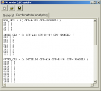
I am in process of creating my own utility for dumping pals
That's great!!
Would that be able to dump the N64 GameShark GAL? It's quite different from normal PAL ICs...
Maybe the SNES GameGenie could, since it seems more standard.
I performed deep analysis of the PAL from my Kid Dracula version (for Famicom)

Generally it agrees with what lidnariq said except one additional discovered register:
$800c - writing any value forces interrupt to be triggered
Here are equations for the chip:
Code:
O6 <= D0 when CPU-!ROMSEL=0 and R/!W=0 and A14=0 and A3=0 and A2=1; --latch
O5 <= D1 when CPU-!ROMSEL=0 and R/!W=0 and A14=0 and A3=0 and A2=1; --latch
02 <= 0 when CPU-!ROMSEL=0 and R/!W=0 and A14=1 and A3=1 and A2=1 else --latch
1 when CPU-!ROMSEL=0 and R/!W=0 and A14=1 and A3=1 and A2=0;
!IRQ! <= 1 when CPU-!ROMSEL=0 and R/!W=0 and A14=1 and A3=0 and A2=1 else --latch
1 when CPU-!ROMSEL=0 and R/!W=0 and A14=1 and A3=1 and A2=1 else
0 when (CPU-!ROMSEL!=1 or R/!W=1) and IRQ_PEN = 1 else
0 when CPU-!ROMSEL=0 and R/!W=0 and A14=0 and A3=1 and A2=1
CLR <= not O2 or IRQ_PEN
CIRAM <= 0 when O6=0 and O5=1 else
1 when 06=1 and 05=1 else
VRC-CIRAM
a a a dddd dddd
1 3 2 7654 3210
4
-----------------
$8004 0 0 1 [.... ..mm] mm - mirroring (source of ciram) (0/1: VRC-CIRAM, 2:GND, 3: VCC)
$800c 0 1 1 [.... ....] writing any value forces interrupt to be triggered
$c004 1 0 1 [.... ....] writing any value acknowledges pending interrupt
$c008 1 1 0 [.... ....] writing any value resets counter from clear
$c00c 1 1 1 [.... ....] writing any value holds counter in clear & acknowledges pending interrupt
* counter is automatically cleared when interrupt becomes pending
* interrupt is triggered when IRQ_PEN=1 and (CPU-!ROMSEL! = 1 or R/!W=1)
Great findings Krzysiobal!
Do your ROMs have the same content as mine?
CRC32
PRG: 6a50b553
CHR: c5d1196e (same as original)
Maybe this was the part of the puzzle that ZxbDragon was needing to finish it's implementation?
Quote:
Do your ROMs have the same content as mine?
Yes
Fisher wrote:
Great findings Krzysiobal!
Do your ROMs have the same content as mine?
CRC32
PRG: 6a50b553
CHR: c5d1196e (same as original)
Maybe this was the part of the puzzle that ZxbDragon was needing to finish it's implementation?
no finish,Krzysiobal info,I try.
没有成功,Krzysiobal信息,我会尝试。
Of course FCEU has ability to track PPU bus, otherwise mappers like MMC2 would not be implemented.
I did my own mapper implementation for Pirate Kid Dracula and it works fine (just there is one quirk - when implementing counter at 86, status bar is switched too late, implementing at 84 seems to be most accurate (should be 83.5 because it is fired in middle of scanline, while in real hardware - almost at end)
Maybe you do it wrong because u assume that when counter reaches 86, it's clocking is stopped?
Analyzing the PAL - reaching 86 makes IRQ_PEN = 1 which makes
CLR <= not O2 or IRQ_PEN
equal to 1 and thus resets counter, but if counter is now reset, AND gate returns 0 (so IRQ_PEN=0) and then CLR=0 so counter is no longer being cleared, so it starts counting from beginning.
https://youtu.be/5hQucuRMnRQCode:
#include "mapinc.h"
static int prg[2];
static int mirr;
static int chr[8];
static int last_pa13;
static int counter;
static int pal_mirr;
static int counter_canclock;
static SFORMAT StateRegs[] =
{
{ 0 }
};
//shifts bit from position `bit` into position `pos` of expression `exp`
#define shi(exp, bit, pos) \
((((exp) & (1 << (bit))) >> (bit)) << (pos))
static void M272Hook(uint32 A) {
int pa13 = (A >> 13) & 1;
if ((last_pa13 == 1) && (pa13 == 0)) {
if (counter_canclock) {
counter++;
if (counter == 84) {
counter = 0;
X6502_IRQBegin(FCEU_IQEXT);
}
}
}
last_pa13 = pa13;
}
static int vrc_addr_mix(int A) {
//this game wires A0 to VRC_A0 and A1 to VRC_A1
return (A & 0xf000) | shi(A, 0, 0) | shi(A, 1, 1);
}
static void Sync(void) {
setprg8(0x8000, prg[0]);
setprg8(0xa000, prg[1]);
setprg16(0xc000, -1);
for (int i = 0; i < 8; ++i) {
setchr1(0x400 * i, chr[i]);
}
switch (pal_mirr) {
case 2: setmirror(MI_0); break;
case 3: setmirror(MI_1); break;
default:
switch (mirr) {
case 0: setmirror(MI_V); break;
case 1: setmirror(MI_H); break;
}
}
}
static DECLFW(M272Write) {
//writes to VRC chip
switch (vrc_addr_mix(A)) {
case 0x8000:
case 0x8001:
case 0x8002:
case 0x8003:
prg[0] = V;
break;
case 0xA000:
case 0xA001:
case 0xA002:
case 0xA003:
prg[1] = V;
break;
case 0x9000:
case 0x9001:
case 0x9002:
case 0x9003:
mirr = V & 1;
break;
case 0xb000: chr[0] = (chr[0] & 0xF0) | (V & 0xF); break;
case 0xb001: chr[0] = (chr[0] & 0xF) | ((V & 0xF) << 4); break;
case 0xb002: chr[1] = (chr[1] & 0xF0) | (V & 0xF); break;
case 0xb003: chr[1] = (chr[1] & 0xF) | ((V & 0xF) << 4); break;
case 0xc000: chr[2] = (chr[2] & 0xF0) | (V & 0xF); break;
case 0xc001: chr[2] = (chr[2] & 0xF) | ((V & 0xF) << 4); break;
case 0xc002: chr[3] = (chr[3] & 0xF0) | (V & 0xF); break;
case 0xc003: chr[3] = (chr[3] & 0xF) | ((V & 0xF) << 4); break;
case 0xd000: chr[4] = (chr[4] & 0xF0) | (V & 0xF); break;
case 0xd001: chr[4] = (chr[4] & 0xF) | ((V & 0xF) << 4); break;
case 0xd002: chr[5] = (chr[5] & 0xF0) | (V & 0xF); break;
case 0xd003: chr[5] = (chr[5] & 0xF) | ((V & 0xF) << 4); break;
case 0xe000: chr[6] = (chr[6] & 0xF0) | (V & 0xF); break;
case 0xe001: chr[6] = (chr[6] & 0xF) | ((V & 0xF) << 4); break;
case 0xe002: chr[7] = (chr[7] & 0xF0) | (V & 0xF); break;
case 0xe003: chr[7] = (chr[7] & 0xF) | ((V & 0xF) << 4); break;
default:
break;
}
//writes to PAL chip
switch (A & 0xC00C) {
case 0x8004: pal_mirr = V & 3; break;
case 0x800c: X6502_IRQBegin(FCEU_IQEXT); break;
case 0xc004: X6502_IRQEnd(FCEU_IQEXT); break;
case 0xc008: counter_canclock = 1; break;
case 0xc00c: counter_canclock = 0; counter = 0; X6502_IRQEnd(FCEU_IQEXT); break;
}
Sync();
}
static void M272Power(void) {
SetWriteHandler(0x8000, 0xFFFF, M272Write);
SetReadHandler(0x8000, 0xFFFF, CartBR);
Sync();
last_pa13 = 0;
counter = 0;
}
static void M272Reset(void) {
last_pa13 = 0;
counter = 0;
Sync();
}
void Mapper272_Init(CartInfo *info) {
info->Power = M272Power;
info->Reset = M272Reset;
PPU_hook = M272Hook;
AddExState(&StateRegs, ~0, 0, 0);
}
