Hi folks, long time no see.
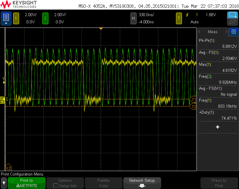
I've got a RP2A03 that I'm quite sure is legit, I just didn't test it thoroughly yet; according to its description it comes from an arcade game. I did one basic test, that is to put some clock in and look at M2, and I get a square wave at 1/12 the input frequency, but with a duty cycle of 75%: 3 cycles down, 9 cycles up, changes state when clock goes from high to low. Now the wiki mentions that M2 should have a duty cycle of 5/8 on the 2A03, could this be another difference between the revisionless 2A03 and the widespread RP2A03G? I would like to have that confirmed by others (I know kevtris and possibly Memblers have a bunch of those arcade 2A03s, I'm looking at you eheh). Note: RST, NMI and IRQ are pulled high, TST is pulled low.
Bonus: I gathered an RP2A03E, which I was less confident that it's legit, and indeed, it is not: M2 is 16 times slower than the input clock. In fact, it looks like it's acting like a 2A07, M2 has a 19/32 duty cycle. I guess this chip will have the square wave's duty cycles and/or DPCM wrong.
Attachment:
 RP2A03_M2_vs_CLK.png [ 61.53 KiB | Viewed 3546 times ]
Attachment:
 fake_RP2A03E_M2_vs_CLK.png [ 61 KiB | Viewed 3546 times ]
Interesting, I didn't knew that there are that kind of timing differences in official chips.
The NOAC vs Famicom compatibility issue in the
Fong Shen Bang - Zhu Lu Zhi Zhan (Mapper 246) thread might be related to M2, too.
Are there some CPU bus timing diagrams for different consoles/chips anywhere? If not, it would be great if somebody could wire a logic analyzer to these pins on a famicom (and/or nes) cart:
M2, R/W, /ROMSEL, A0, D0 and then plug the cart into different consoles & clones and record the timings to see when the separate signals are changing in relation to each other. Having
21MHz logged would be nice, too. But it isn't externally available on the 60pin Famicom slot (only on 72pin NES slot). And I don't know if normal logic analyzers are capable of recording frequencies like 21MHz?
Scope picture would be also great (or even better), though it might need some puzzling to make a complete timing diagram with 2-channel scopes.
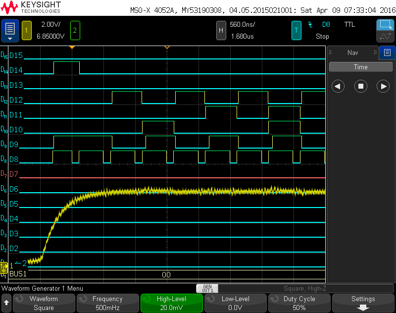
Well, I have 16 logic inputs on the scope I'm using, I was just a bit lazy to go find that ribbon cable and plug it. Besides, sometimes the gory analog details are fun to look at. But the next picture I can get is CLK, M2, D0-7, R/W, A0-A3 and A8 with hardwired (through resistors!) $00 on the databus, if that looks interesting. Note that that thing is on a breadboard.
Would be great! 00h (BRK opcode) should cause enough traffic on databus to see when exactly the CPU is outputting values. With the 00h through resistors (without real data from cartridge) there would something missing - but that could be actually an advantage as it will be more clear what the raw CPU is doing with the databus.
/ROMSEL would be also nice, but it's externally generated via a 74LS139, maybe you reproduce that on the breadboard too (?), or else one could just imagine how /ROMSEL should behave (as far as I understand, it should be LOW when A15 and M2 are both HIGH).
Oh, and what exactly is a RP2A03 (and RP2A03E)? Do you know where that chips came from originally, ie. if they've been used in NES or Famicoms, or clones, or arcade cabinets?
At the moment, I would be mostly interested in the "normal" timing of the official most-common standard NES/Famicom consoles (which, oddly, I couldn't find timing diagrams for it). And of course, in the NOAC clone timings to see if they could explain the behaviour of the Fong Shen Bang cart. But in general, it would be also nice to have timing charts for all kinds of other clones and official chip revisions.
I've talked to kevtris about it and it is confirmed. He had trouble getting the revisionless chip to work with his HDMI upgrade because of the timing difference. He mentioned that M2's timing changes on a DPCM access cycle as well, apparently it's relatively dramatic on the revisionless version.
I've seen at least a couple people on an arcade tech forum (KLOV) mention that on the VS board, if you replace the 2A03 with a 2A03G that TKO Boxing (Ring King) no longer works.
These are the chips I have:
2A03 (VS Unisystem)
2A03E (Playchoice)
2A03E (fake remarked one)
2A03G (front-loader)
2A03H (top-loader)
I have one of the PAL UMC chipsets as well, I forget the part number at the moment.
I have .1" headers soldered to the back of the NES CPU on my NES board, that's what I've been using for test connections. Currently I'm in the middle of re-arranging my basement, partly with the goal of setting up an area where my NES, scope, TV, and a PC can be in the same area. After I've got this setup ready, if it helps, I could also log some data.
The RP2A03 I have comes from an arcade, according to the seller, though I don't know which one. The RP2A03E comes from a Chinesse seller, and I took a chance when buying it because I knew it could possibly be fake, and it was indeed.
Memblers: now that's interesting, M2 would change on DPCM DMA access. I wonder if it changes with $4014 DMA, too. I'm in a state that I need RAM to do anything useful, and that may take a bit of time. Anyway the next step is to get chronograms of various 2A03 pins during repeated execution of BRK.
RAM and not ROM?
Alternatively, I remember a project that deliberately treats the 6502 as a coprocessor, and an atmega feeds it φ0 and data lines. The 2A03 should be ok being underclocked all the way down to 120kHz (instead of its normal 21.5MHz) because the 6502 die inside is "safe" down to 10kHz.
RAM at $0000-$3FFF and "RAM" at $8000-$FFFF, the latter not writable by the 2A03 but instead by some devboard controlling RST, R/W and the entire address/data bus (a bit like an EPROM emulator). Hey, I just thought that I can use that devboard to control NMI and IRQ too. Anyway, that way I can run the core at full speed (CLK = 21.47727MHz) and get "actual" timings.
But you don't need to. You can still calculate how things would work at full speed given data from underclocking: you can separate out the timing into analog effects (slew rate, output driver conductivity, parasitic capacitance) and digital effects.
Plus, by underclocking, you can use a dramatically less capable oscilloscope to find out what the timing is.
Anyway, the bit where the 2A03x puts all its drivers in HiZ mode when in reset means that you could also use another microcontroller to pre-load the contents of RAM ... or is that already what you were planning on doing?
lidnariq wrote:
Anyway, the bit where the 2A03x puts all its drivers in HiZ mode when in reset means that you could also use another microcontroller to pre-load the contents of RAM ... or is that already what you were planning on doing?
Exactly. I have a nice devboard I can turn easily into a UART (usb-cdc) EPROM emulator. Programming RAM would only require to hold reset on 2A03, drive the buses to program said RAM, undrive buses, and release reset.
So, here's a couple of pictures.
Signals for all pictures:
D0-D7: Databus, also seen on BUS1
D8: CLK
D9: R/W
D10-D13: A0-A3
D14: A8
D15: A15
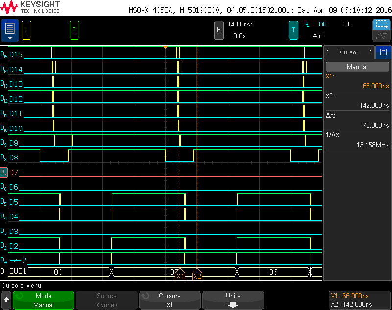
Timing of R/W: (For now, ignore BUS1)
Attachment:
File comment: Timing of R/W
 scope00.png [ 26.66 KiB | Viewed 3214 times ]
It appears that R/W go low faster than I goes high; suprisingly the databus goes HiZ before R/W goes high. The address lines all transition somewhat at the same time, ~66ns after M2 falls, pretty much at the same time that R/W can go low, but it takes 142ns to R/W to go high. It seems the higher address bits changes a bit before the lower ones, though it can be because of different characteristics of the circuit (different parasitic capacitance?) so it should be determined with a known load.
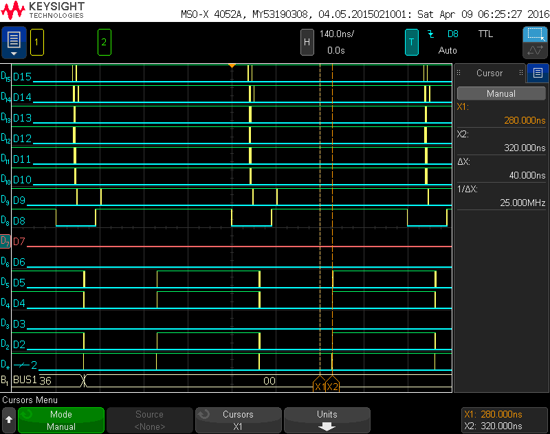
Timing of writes on the databus: (For now, ignore BUS1)
Attachment:
File comment: Timing of writes
 scope01.png [ 26.43 KiB | Viewed 3214 times ]
Databus changes ~40ns after half the period of M2. This support what is written on the wiki: M2 is likely not to be used internally by the 6502 core (that is, M2 ≠ φ2), rather, φ2 is derived from clock independently of M2 and is a 50% duty cycle square wave.
(Goto "real fun" below to see something actually interesting)
Behavior of reset:
Attachment:
File comment: Reset
 scope02.png [ 22.39 KiB | Viewed 3209 times ]
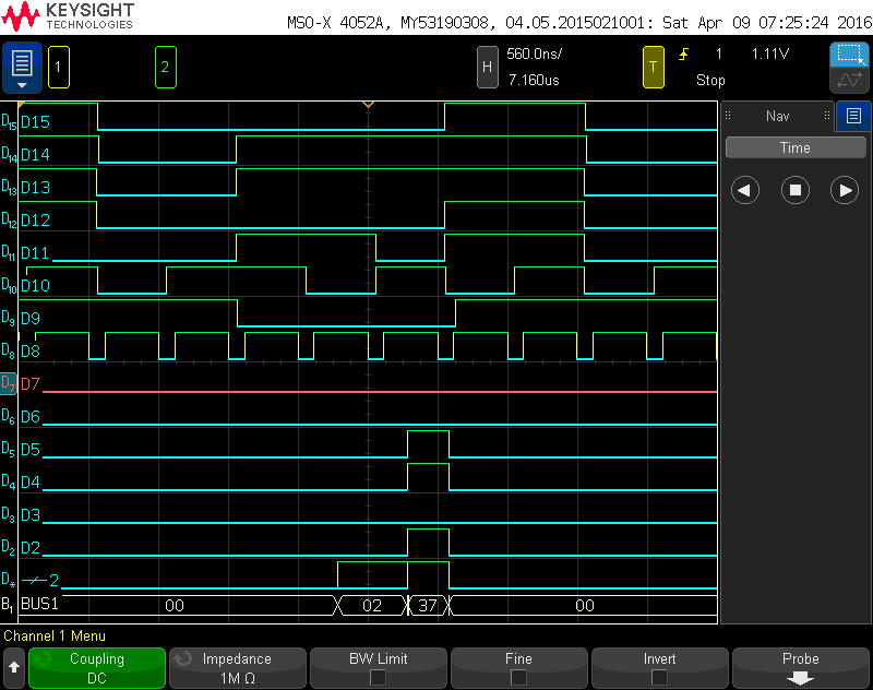
Pretty standard. M2 has a first slightly truncated clock, then goes on normally. The core seems to do nothing for 4 cycles, (can't determine fully the address read), then does the dummy "pushes" (A15 = 0, A8 = 1, R/W = 1) and read the RESET vector ($FFFC-D) then it fetches BRK.
Attachment:
File comment: Reset (suite)
 scope03.png [ 23.27 KiB | Viewed 3209 times ]
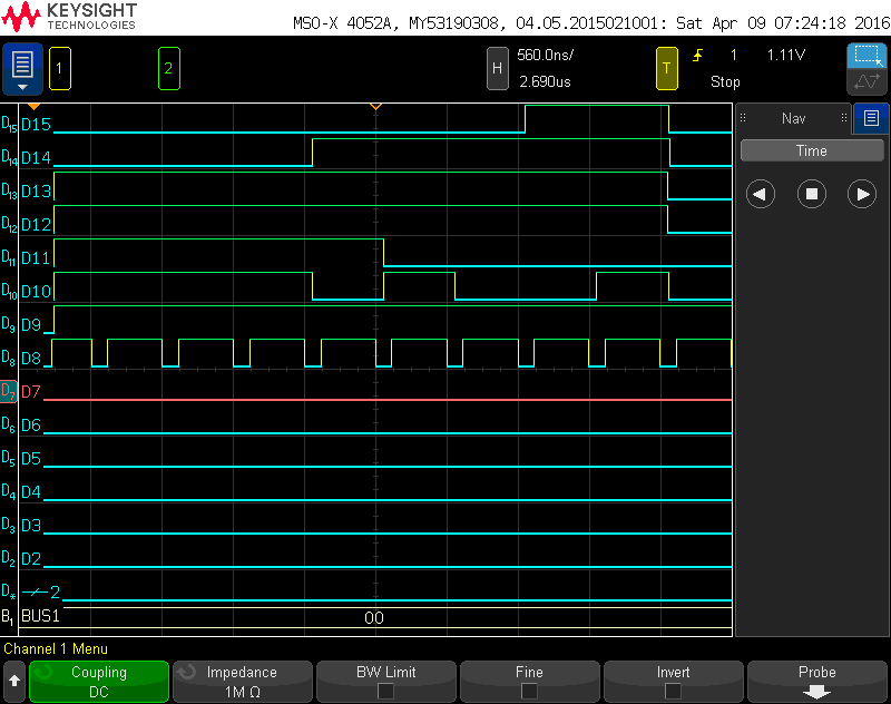
Execution of BRK. The core fetches BRK, the second byte, then pushes $0002 as return address, and $37 as status byte, then fetches the IRQ vector ($FFFE-F) and then it goes on forever. The first push is at $01?B, right after the last dummy push from reset, and the status byte is B = I = Z = 1 (the unimplemented bit is obviously set). Across several resets, I get the Z flag either set or clear, but the others seem to be always clear.
Now the real fun begins here:Attachment:
File comment: Bug in Reset
 scope05.png [ 32.75 KiB | Viewed 3209 times ]
The yellow trace is the RESET signal. It is controlled by an digitally controlled solid state analog switch. The signal is pretty clean and had no glitches whatsoever, only a bit of noise. At some point I put the switch off (goes HiZ) and RESET floats to 5V through a 2K resistor. Even with this clean RESET signal the RP2A03 does something strange here: it seems to be performing a sprite DMA straight out of reset. This happens reliably when I power up the chip while RESET is low, then I release it after some time, even if it's after a few seconds. Notice how it quickly alternates between reads and writes, and writes are at 0xxxxxx0xxxx0100, most likely $2004. This chip has a buggy reset, and at power up it seems to do a sprite DMA. The other resets after power up are fine however, that sprite DMA is gone and the core behave normally; I took the other screen captures of this post after a subsequent reset, otherwise I get something like this instead.
Another difference spotted: the TST pin is likely to be Not Connected, it seems to do nothing and does not even have protection diodes. I tested other pins to be sure, I can sink 1mA with only ~.5V below ground on a Hi-Z pin and that didn't happen with the TST pin at -1V, no current.
Are there people out there willing to lend me their RP2A03s? I would pay for shipment. With the things I find, I would rather not write info into the wiki with only one sample. The sprite DMA on POR bug is especially strange and I want to know if it's not just my chip.
The original 2A03 documentation mentioned a crystal oscillator from pins 29 to 30.
Also, there's the
decapped 2A03 with its broken IRQ generator that Quietust put into its own
simulator
lidnariq wrote:
The original 2A03 documentation mentioned a crystal oscillator from pins 29 to 30.
Also, there's the
decapped 2A03 with its broken IRQ generator that Quietust put into its own
simulatorThe actual die shots of that chip are available
here (don't worry, it's not a private link - you can navigate there from the root of siliconpr0n.org) - it's not delayered, but it should still be good enough quality to trace out basic stuff like the clock divider (and compare it to Visual2A03).
Jahrmander, maybe I could loan you my 2A03. If you still need one, PM me your address to me.
Not on the revision-less one, but one interesting thing I noticed on that TST pin is that it's actually used on the Playchoice where it's called "SPECIAL". The PC10 schematic calls for RP2A03E.
Huh, the schematic there shows that /SPECIAL goes high after the 2A03's /NMI has been asserted for 5 M2 cycles...
Quietust wrote:
lidnariq wrote:
The original 2A03 documentation mentioned a crystal oscillator from pins 29 to 30.
Also, there's the
decapped 2A03 with its broken IRQ generator that Quietust put into its own
simulatorThe actual die shots of that chip are available
here (don't worry, it's not a private link - you can navigate there from the root of siliconpr0n.org) - it's not delayered, but it should still be good enough quality to trace out basic stuff like the clock divider (and compare it to Visual2A03).
Hmm I can't make any sense of the die shot (or any other die shots whatsoever), so it won't help me... maybe if I find some doc on how to understand them.
I just saw on the VS System schematic, it's a 2A03 and that pin 30 is named "NC" and is grounded. That what I observed on the chip indeed.
lidnariq wrote:
Huh, the schematic there shows that /SPECIAL goes high after the 2A03's /NMI has been asserted for 5 M2 cycles...
It's a bit special, considering it takes at least 7 cycles to serve any interrupt.
Jarhmander wrote:
lidnariq wrote:
Huh, the schematic there shows that /SPECIAL goes high after the 2A03's /NMI has been asserted for 5 M2 cycles...
It's a bit special, considering it takes at least 7 cycles to serve any interrupt.
Right, but it stays high forever after. I don't know why they bothered with the special logic for "5 cycles after /NMI asserted", but if the 2A03E has the same self-test mode that the 2A03G does (I doubt it), then maybe the intent was that the game could test that the sound hardware worked, and then enable the video kernel?
Jarhmander wrote:
I just saw on the VS System schematic, it's a 2A03 and that pin 30 is named "NC" and is grounded. That what I observed on the chip indeed.
In the RP2A03, pin 30 is not connected to anything at all internally, so "NC" is correct.