First off: Hello nesdev community! I have used the wiki and read many posts here which greatly helped understandindg the way an NES/Famicom works. Now I want to give something back, whether it be useful or not.
This is a Proof of Concept on expanding the MMC3s Addressbus by one Bit, so it can address an actual 1MB of PRG data, or 128 Banks. I saw a post here which assigned TXROM type to a PCB, which does support 2MB of ROM data, but it doesnt have true Bank support for more than 64 Banks, it just writes to some latch which controls ROM lines and a switch to switch in a game that has 512kB PRG max.
The reason why I did this was because I got stuck in another project, and I kind of got carried away when I thought it would be awesome to play some MegaMan Minus Infinity on real Hardware without chopping up the rare MMC5 NES cartridges (I might have gotten myself a Famicom version of an MMC5 cart with an adapter, but that would have cut out the fun and INL Boards dont seem to support either MMC3 with 1MB PRG nor MMC5 at all).
My circuit consists of "only" 10 discrete Logic ICs, this can actually be cut by a bunch of ICs (I used stuff laying around, which resulted in using NAND gates to get a simple NOT and stuff like that increasing the number of used ICs). Essential were 2 FlipFlops, a Latch, 2 demultiplexer for Address access, an OR-Gate, and a bunch of AND-Gates.
For now I have only the Logic signals to show off which i captured to debug everything, it should be enough to see if the circuit is doing its work or not. It would be helpful if somebody could verify it, i couldnt see any malfunction.
The code used to test the circuit:
A.bmp [ 3.29 MiB | Viewed 5105 times ]
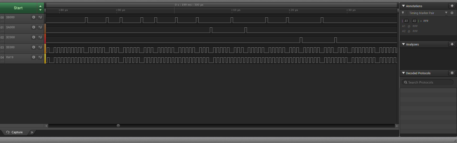
Picture A:
B.bmp [ 3.18 MiB | Viewed 5105 times ]
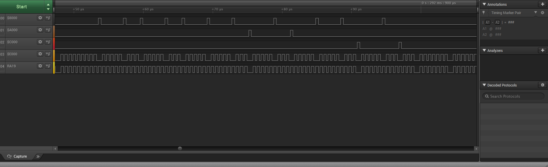
Picture B:
Note: $8000, $A000, $C000, $E000 show the access (so Read and Write) to the specific Address area (8kB Bank). RA19 would be connected to PRG ROMs A19. the first time $8000 is pulled High on the pictures is the first "sta $8000" instruction. The whole code is executed from $E000-$FFFF, so reads from $E000-$FFFF always pull RA19 high, resulting in the last Bank always being switched in.
I have yet to draw an exact schematic for everything, and test it with the actual game (I ordered the proper parts already).
This is a Proof of Concept on expanding the MMC3s Addressbus by one Bit, so it can address an actual 1MB of PRG data, or 128 Banks. I saw a post here which assigned TXROM type to a PCB, which does support 2MB of ROM data, but it doesnt have true Bank support for more than 64 Banks, it just writes to some latch which controls ROM lines and a switch to switch in a game that has 512kB PRG max.
The reason why I did this was because I got stuck in another project, and I kind of got carried away when I thought it would be awesome to play some MegaMan Minus Infinity on real Hardware without chopping up the rare MMC5 NES cartridges (I might have gotten myself a Famicom version of an MMC5 cart with an adapter, but that would have cut out the fun and INL Boards dont seem to support either MMC3 with 1MB PRG nor MMC5 at all).
My circuit consists of "only" 10 discrete Logic ICs, this can actually be cut by a bunch of ICs (I used stuff laying around, which resulted in using NAND gates to get a simple NOT and stuff like that increasing the number of used ICs). Essential were 2 FlipFlops, a Latch, 2 demultiplexer for Address access, an OR-Gate, and a bunch of AND-Gates.
For now I have only the Logic signals to show off which i captured to debug everything, it should be enough to see if the circuit is doing its work or not. It would be helpful if somebody could verify it, i couldnt see any malfunction.
The code used to test the circuit:
Attachment:
A.bmp [ 3.29 MiB | Viewed 5105 times ]
Code:
;test $8000, mode 0:
lda #$06;switch $8000, mode 0
sta $8000
lda #$00
sta $8001
lda $8000;not from RA19
lda #$40
sta $8001
lda $8000;should be from RA19
;test $A000, mode 0:
lda #$07;switch $A000, mode 0
sta $8000
lda #$00
sta $8001
lda $A000;not from RA19
lda #$40
sta $8001
lda $A000;should be from RA19
;test $C000, mode 0:
lda #$06;switch $C000, mode 0, should switch $8000
sta $8000
lda #$00
sta $8001
lda $C000;should be from RA19
lda #$40
sta $8001
lda $C000;should be from RA19
Attachment:
B.bmp [ 3.18 MiB | Viewed 5105 times ]
Picture B:
Code:
;test $8000, mode 1:
lda #$46;switch $8000, mode 1, should switch $C000
sta $8000
lda #$00
sta $8001
lda $8000;should be from RA19
lda #$40
sta $8001
lda $8000;should be from RA19
;test $A000, mode 1:
lda #$47;switch $A000, mode 1
sta $8000
lda #$00
sta $8001
lda $A000;not from RA19
lda #$40
sta $8001
lda $A000;should be from RA19
;test $C000, mode 1:
lda #$46;switch $C000, mode 1
sta $8000
lda #$00
sta $8001
lda $C000;not from RA19
lda #$40
sta $8001
lda $C000;should be from RA19
Note: $8000, $A000, $C000, $E000 show the access (so Read and Write) to the specific Address area (8kB Bank). RA19 would be connected to PRG ROMs A19. the first time $8000 is pulled High on the pictures is the first "sta $8000" instruction. The whole code is executed from $E000-$FFFF, so reads from $E000-$FFFF always pull RA19 high, resulting in the last Bank always being switched in.
I have yet to draw an exact schematic for everything, and test it with the actual game (I ordered the proper parts already).