The information on the NESDEV WIKI about the registers of INES Mapper 052 is wrong
Here is the correct information :
$6000-7FFF
D7.... ....D0
ABCD EFGH
A (D7) : LATCH [0:En 1:Dis]
B (D6) : CHR Size [0:256 1:128]
C (D5) : CHR bit 1
D (D4) : CHR bit 0
E (D3) : PRG Size [0:256 1:128]
F (D2) : PRG bit 2 + CHR bit 2
G (D1) : PRG bit 1
H (D0) : PRG bit 0
*************************************************************
And here are some older info about mapper 52 :
*************************************************************
Mario 7 in 1
7 bit 0
---------
xABC DEFG
x- not used
A- CHR ROM bank size. 1=128K, 0=256K
D- PRG ROM bank size. 1=128K, 0=256K
G- PRG ROM bank "part" (for 128K banks)
E,F- PRG ROM 256K bank
*************************************************************
Registers of Gold 7 in 1 HIK AR456
1000 0000
1110 1010
1111 1011
1100 1100
1101 1101
1110 1110
1111 1111
*************************************************************
Registers of 1997 SUPER HIK 8 IN 1 EW-800
1101 1000
1100 1001
1110 1010
1111 1011
1100 1100
1101 1101
1110 1110
1111 1111
*************************************************************
From #nesdev IRC :
[19:35] <thefox> XACCYBPP
[19:35] <thefox> BPP = 3 bit PRG bank selection, selects a 128K prg bank
[19:35] <thefox> Y = PRG size selection, 0 = 256, 1 = 128
[19:35] <thefox> BCC = 3 bit CHR bank selection, selects a 128K prg bank
[19:35] <thefox> A = CHR size selection, 0 = 256, 1 = 128
[19:35] <thefox> X = always 1
*************************************************************
For emulation
Cbank = (E*4 + B*2) OR (A and C) OR (!A and MMC3C)
BTW, bit7 of the extra banking register is used for locking further bankswitching, games doing this when using SRAM area in case tot interfere with the running program...
the same way, bit7 of A001 register of MMC3 used to enable banking at the cartridge start...
anyway, there isn't much useful for emulation, since actually can beignored
*************************************************************
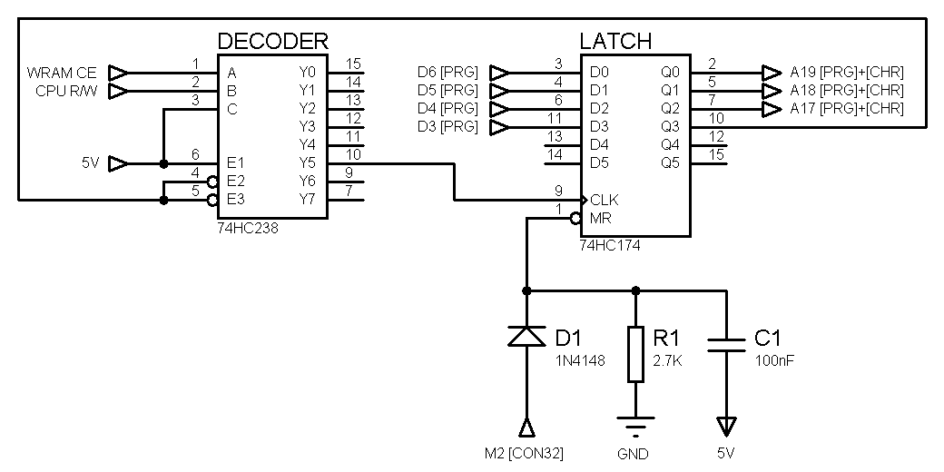
It is possible to remake this kind of cartridge by using 74HC161 as a latch
Here is the correct information :
$6000-7FFF
D7.... ....D0
ABCD EFGH
A (D7) : LATCH [0:En 1:Dis]
B (D6) : CHR Size [0:256 1:128]
C (D5) : CHR bit 1
D (D4) : CHR bit 0
E (D3) : PRG Size [0:256 1:128]
F (D2) : PRG bit 2 + CHR bit 2
G (D1) : PRG bit 1
H (D0) : PRG bit 0
*************************************************************
And here are some older info about mapper 52 :
*************************************************************
Mario 7 in 1
7 bit 0
---------
xABC DEFG
x- not used
A- CHR ROM bank size. 1=128K, 0=256K
D- PRG ROM bank size. 1=128K, 0=256K
G- PRG ROM bank "part" (for 128K banks)
E,F- PRG ROM 256K bank
*************************************************************
Registers of Gold 7 in 1 HIK AR456
1000 0000
1110 1010
1111 1011
1100 1100
1101 1101
1110 1110
1111 1111
*************************************************************
Registers of 1997 SUPER HIK 8 IN 1 EW-800
1101 1000
1100 1001
1110 1010
1111 1011
1100 1100
1101 1101
1110 1110
1111 1111
*************************************************************
From #nesdev IRC :
[19:35] <thefox> XACCYBPP
[19:35] <thefox> BPP = 3 bit PRG bank selection, selects a 128K prg bank
[19:35] <thefox> Y = PRG size selection, 0 = 256, 1 = 128
[19:35] <thefox> BCC = 3 bit CHR bank selection, selects a 128K prg bank
[19:35] <thefox> A = CHR size selection, 0 = 256, 1 = 128
[19:35] <thefox> X = always 1
*************************************************************
For emulation
Cbank = (E*4 + B*2) OR (A and C) OR (!A and MMC3C)
BTW, bit7 of the extra banking register is used for locking further bankswitching, games doing this when using SRAM area in case tot interfere with the running program...
the same way, bit7 of A001 register of MMC3 used to enable banking at the cartridge start...
anyway, there isn't much useful for emulation, since actually can beignored
*************************************************************
It is possible to remake this kind of cartridge by using 74HC161 as a latch
