This mapper is used by two games:
- 蝶變 (Diébiàn, in most ROM sets nonsensically rendered in Japanese as "Chou Hen"), the original Joy Van version of Galactic Crusader, overall CRC32 B550B627
- 未来小子 (Wèilái Xiǎozi), the original Joy Van version of Metal Fighter µ, overall CRC32 CEC28502
The unaltered ROM image of Diébiàn can be found as "Incantation (Dip Bin) (Joy Van)" in GoodNES v3.23b and is incorrectly set to Mapper 146, causing it to reset when pressing Start because of a simple copy protection.
FCEUX and Nestopia use the value written to $4102 plus three as the 8K CHR ROM bank. That is good enough for Wèilái Xiǎozi, but not for Diébiàn. The actual bank seems to be not $4102 plus a fixed "plus three", but "plus number of previous $4100 writes since the last $4101 write", which just happens to be three in the case of Wèilái Xiǎozi.
Attached find a Nintendulator Mapper source file which runs both games in their unaltered form. Edit: See end of thread for updated source files.
... That sounds
extremely similar, but not identical, to how I discovered that
Mapper 36 actually works.
viewtopic.php?f=9&t=15302HI,NewRisingSun , help me,thank you.
I have updated my Mapper 136 source file on the assumption that it's like Mapper 36, only with CHR. Before, I was applying the RR value to CHR immediately after any $4100-$4103 write, instead of waiting for the $8000-$FFFF write. (This would obviously be fatal for a PRG switch.) Diébiàn and Wèilái Xiǎozi both indeed finish their bankswitching code with a write to $FFFF, which mystified me before I learned about Mapper 36.
If Mapper 36 did not have that simplified CHR ROM switch at $4200, one could maybe even have merged mappers 36 and 136. While the "start RR" value for PRG is loaded into bits 4 and 5 of $4102 in Mapper 36, the "start RR" value for CHR is loaded into bits 0 and 1 of $4102 in Mapper 136.
Edit: Forgot a break in a switch statement.
Even if the ASIC is the same, the connections to the card edge look like they'll differ in an incompatible way...
But, yeah, I'll take a look at what the other three lines were intended to be. Since both Policeman and Strike Wolf include that write to $4101 I really have to wonder if i made an experimental error in claiming that writes to $4101 had no visible effect, or if it's a difference between the upper and lower nybbles of the IC, or if it's just a different IC altogether.
Debugging Pūkè Jīnglíng (the original version of Peek-a-Boo Poker), it seems that $4101 is a XOR mask that is applied to the value written to $4102 afterwards. I noticed that when I set that game to Mapper 136, my previous emulation selected the correct CHR bank when 00 was written to $4101, and the wrong CHR bank when FF was written to $4101, and the code does EOR the bank number in a similar fashion when writing FF to $4101. Attached find another update to Mapper136.cpp that incorporates this change.
With this $4101 behavior emulated, Pūkè Jīnglíng now runs at mapper 136 as well, though it also had CNROM compatibility code (provided that the CNROM emulation did NOT emulate bus conflicts). The game also writes to $4104, but as I understand the board's address mask, that should just be an alias for $4100 (it writes to $4104 in "direct CHR" mode and to $4104 in "CHR increment" mode). The same applies to the
initial AVE release of F-15 City War (overall CRC32 88A6B192), though the address mask before comparison needs to be $E123 rather than $E103 (so that $4120 is NOT an alias for $4100), otherwise the NINA-03 compatibility write will interfere. (That particular ROM is strange --- it reads from $4100 to check if the current register has the correct value, quite similar to the Diébiàn/Wèilái Xiǎozi, but then ignores the result. I wonder if AVE just hacked the NINA-03 compatibility code into the mapper 136-targeted ROM image?)
Can you check whether writing FF to $4101 has a similar effect on the Mapper 36 board?
Edit: I noticed that this $4101-aware emulation of Mapper 136 also covers all games (Xiǎo Mǎlí Nei-Hu version, Mahjong Block Super Mega version) of Mapper 173, including the protection. It seems like FCEUX' mapper 173 emulation is a special case emulation for two games, whereas Mapper 136 as described is the general case, as Diébiàn and Wèilái Xiǎozi do not work under Mapper 173.
Mapper 172 (that silly Horse Racing game)'s protection read is passed as well, but the CHR bank is visibly wrong. Apparently, that game uses bits 4 and 5 instead of bits 0 and 1 for the CHR bank number, and messes up the order a bit. Probably the same IC but connected differently. Lastly, there is also Mapper 132 (Qiwang), which uses bits 0 and 1 for CHR, and bits 2 and 3 for PRG bank. Again, probably just a case of connecting the same IC in a different way.

I'd say look at the source code.
Oh wait: Now I see it. The name "
Diébiàn" must be some off-brand knockoff without any sort of
free software guidelines.
NewRisingSun wrote:
I wonder if AVE just hacked the NINA-03 compatibility code into the mapper 136-targeted ROM image?)
Almost guaranteed.
Quote:
Can you check whether writing FF to $4101 has a similar effect on the Mapper 36 board?
The answer is "ew".
Doing my best to augment the contents of the m36 wiki page for what the full IC seems to do:
Code:
read $4100-$4103: [.RRR .XXX] - shows internal state; XXX←CCC⊕xxx
write $4100: When M=0, copy (PPP⊕yyy) to RRR; when M=1, RRR++ and also CCC++
write $4101: [.xxx .yyy] - XOR values
write $4102: [.PPP .CCC] - request 32 KiB PRG and 8KiB CHR
write $4103: [...M ....] - load-vs-increment mode (yes, still the upper nybble only)
write $8000-$FFFF: copy RRR and XXX to PRG and CHR banking pins
Take my results with a huge grain of salt... only pin 23 acts like CHR A13; pin 22 is always high no matter what I write. It could well be that this instantiation of the IC is buggy, which is why this PCB adds a 74'138 and 74'175. I can see the amount of current being sourced out of pin 22 changing (LED is changing brightness) depending on values written.
Pin 24 is really daft: you can only toggle it by loading the right value into RRR, and incrementing it until PRG A18 toggles. I haven't yet found a way to set it to a known value.
The full intended pinout seems to be
Code:
.--\/--.
PRG A17 <- |01 24| -> PRG A18 (yes really)
PRG A16 <- |02 23| -> CHR A13
PRG A15 <- |03 22| -> always high
GND ?? |04 21| <- CPU A13 (rn)
5V ?? |05 20| <- CPU A14 (rn)
CPU D0 <> |06 19| ?? GND
5V ?? |07 18| <- CPU R/W (n)
CPU D1 <> |08 17| <- /ROMSEL (rn)
CPU D2 <> |09 16| <- M2 (n)
CPU D6 <> |10 15| <- CPU A8 (rn)
: :
If someone from Taiwan can provide us boards containing the real TCU-02 IC, that would probably be pleasant in figuring out what the hell this thing might actually do and if it's supposedly like your pinout. FYI, there are two versions of Joy Van's Weilaixiaozi; one with fudgy scanline timer code, causing the title screen to jitter, supplied as regular CNROM. The other one appears to be a later revision that uses the supposed TCU-02 board logic. This later revision also fixes the title screen issues.
There's a big, fat "ASLIC AX-24G" IC on my friend's Master Chu cart, and from a glance it doesn't appear to match your supposed pinout though, so that's irrelevant to the whole discussion. I can provide actual pictures if anyone wants to take a look at it, though.
Pictures of rare PCBs are always appreciated, even if we can't do anything with them yet.
Here you go:
The rest of the PCB's he has of some Sachen stuff is on his flickr page, including Rocman X
(which seems to be wired up to a weird CHR ROM and CHR RAM variant, despite not showing any instance of Chinese text boxes in the game at all?)https://www.flickr.com/photos/153392699 ... 2682439086
"Rare"? "CHR ROM and CHR RAM without hanzi"? You don't need Sachen for that.
High Speed (TQROM, mapper 119)Back to topic:
Perhaps it was originally planned to have a Chinese version, but that was cut late. Or perhaps it shares an engine with a game that uses a combination because it uses Chinese text.
Or the engine uses a combination because it was more convenient. I was lead programmer for
The Curse of Possum Hollow, which has a 62256 (32Kx8 SRAM) for CHR RAM. But if only 8Kx8 SRAMs were available, it would probably have used a setup analogous to TQROM. The level backgrounds are in CHR RAM banks 0-7, with the playfield in 0-3 and the repeating parallax strips in 4-7. These have to be in CHR RAM because they're replaced a tile at a time as the camera proceeds through each level. Banks 16-31 are used for sprites, which are always loaded into CHR RAM a whole bank at a time. Banks 8-15 are used for static background things, primarily text fonts.
Huh. Given that picture, it's more likely that the "ASLIC AX-24G" actually connects to D0-D5, not D0-D2 and D4-D6.
kazblox wrote:
FYI, there are two versions of Joy Van's Weilaixiaozi; one with fudgy scanline timer code, causing the title screen to jitter, supplied as regular CNROM. The other one appears to be a later revision that uses the supposed TCU-02 board logic. This later revision also fixes the title screen issues.
The opposite is the case: The "CNROM version" is just a mapper hack of the TCU-02 version. You can still see the remnants of the TXC IC writes in it. Because the mapper hardware is written to while the split point is being timed, hacking the mapper code has the side effect of creating a shaky screen split.
kazblox wrote:
There's a big, fat "ASLIC AX-24G" IC on my friend's Master Chu cart, and from a glance it doesn't appear to match your supposed pinout though, so that's irrelevant to the whole discussion.
There is no image of Master Chu with any $4100-$4103 writing code, so that is indeed off-topic. The Joy Van version has code for CNROM and some unknown mapper hardware with two registers at $8000 and $8001 that are not MMC3-compatible, respectively. The Color Dreams version only has support for the Color Dreams latch, and the Sachen version has NINA-03 compatible bankswitching code, plus remnants of Color Dreams' charge pump-driving writes.
Attached source file txc.cpp for Nintendulator combines code for all known TXC board configurations; they are basically different ways of connecting the various lines around the same IC, plus Mapper 36's extra CHR latch. Mapper 173 is identical to Mapper 136, as mentioned before.
I am assuming that lidnariq's description of Mapper 36 has the CPU data bits shifted by four bits. That's a matter of definition, however; one might as well say that Mapper 36 is not shifted and everything else is. I had to deviate from lidnariq's description (or rather my understanding of it) in one way to make this work:
Code:
write $4100: When M=0, copy (PPP⊕yyy) to RRR; when M=1, RRR++ and also CCC++
The "also CCC++" does not correspond with what any game expects. All the games that read from $4100 and use the increase mode assume that only one of the nibbles is increasing.
The source file also includes a summary of the bits used by the various games.
Note! Mahjong Block sometimes selects the wrong CHR bank when the playfield appears for the first time. This error occasionally occurs in other versions of the game as well, even the ones that only have NINA-03 code in them. I therefore attribute this to a game error, not a mapper emulation error.
Edit:
Updated the mapper source files to incorporate recent redumps of the Idea-Tek versions of Puzzle and F-15 City War.
NewRisingSun wrote:
The opposite is the case: The "CNROM version" is just a mapper hack of the TCU-02 version.
So, if the only actual Taiwanese Joy Van release of Weilaixiaozi appears to be using the TCU-02, and the mapper hack is unofficial, I guess the "GS63030-A" chips on Pongba's post represents the actual IC. Joy Van's Mahjong Trap also appears to be using the GS63030-A IC as well, but the current and ONLY dump is using CNROM and thus likely
(I haven't exactly checked yet) a mapper hack.
viewtopic.php?t=2909We REALLY need to organize our dumps, or else crap like this gets lost forever in a swarm of loose .NES files screaming
"hacks, hacks, hacks. NESTIIICCCCLLEEEE!!!! copiers, copiers, hacks, hacks, hacks.".
kazblox wrote:
Joy Van's Mahjong Trap also appears to be using the GS63030-A IC as well, but the current and ONLY dump is using CNROM and thus likely (I haven't exactly checked yet) a mapper hack.
Confirmed. It starts off by writing to $4101, but then only writes to $8000-$FFFF, followed by RTS and some leftover garbage that looks similar to Mapper 136 code in Diebian. I suppose I could try to "unhack" it, but I won't, lest I would contribute to
more hacks flying around.
kazblox wrote:
We REALLY need to organize our dumps,
Theoretically, GoodNES would be the candidate here. Unfortunately it's so badly maintained that it's beyond useless except as a search term for torrents.
So, anyone still in contact with pongbashi?
NewRisingSun wrote:
Unfortunately it's so badly maintained that it's beyond useless except as a search term for torrents.
And this is why I'm adding on to the Sachen stuff in the MAME softlist in private until I'm assured that the dumps are at least good and directly come from the actual ROM chips, or a Kazzo board.
MAME also does a horrible job at documenting Sachen stuff, considering that most of the knowledge in that area derives from GoodNES, but I'm planning to fix a big chunk of that.

OK, my friend has an original Mahjong Trap cart and a Kazzo, yay!

If someone could write Kazzo scripts for all variants of the ASIC described in this thread, that would be great. Currently, I'm at an outing for a few hours, so I won't be able to do much.
I have modified the CNROM dumping script for Mapper 136 (rename extension to .ad). Since I have no Kazzo, I cannot try it; just tell me if it does not work with Mahjong Trap. Mapper136 is the simple version, which should be enough according to my understanding of the IC, otherwise Mapper136a initializes all four registers.
kazblox wrote:
Here you go:
The rest of the PCB's he has of some Sachen stuff is on his flickr page, including Rocman X
(which seems to be wired up to a weird CHR ROM and CHR RAM variant, despite not showing any instance of Chinese text boxes in the game at all?)https://www.flickr.com/photos/153392699 ... 2682439086Needs PPU-accessible RAM to map four nametables. I keep reading that it's one of those that do, but now that we've got someone with the board handy, we should make sure…
Myask wrote:
[Sachen's Rocman X] Needs PPU-accessible RAM to map four nametables. I keep reading that it's one of those that do, but now that we've got someone with the board handy, we should make sure…
The PCB pictures are good enough to successfully trace the 6264's /CE pin to the
NOT PPU A13 signal on the card edge, so that's something.
Rewriting yesterday's remarks now that all Idea-Tek games except for
Venice Beach Volleyball have been redumped. These games share a similar IC (with different markings) as the one described for
Mapper 36. But they are connected in different ways.
Mapper 173This board connects the IC's data bits four bits rotated from the
Mapper 36 description, so $4103's Mode bit is at bit 0, not at bit 4. $4102's D0 (IC Pin 3) is CHR A13, but $4102's D1 is NOT CHR A14. I cannot quite see which pin of the IC is connected to CHR A14 (I'd say Pin 4 or Pin 22), as the lead goes under the chip, but CHR A14 is always the inverse of the IC's XOR flag, e.g. a XOR flag of 1 selects CHR banks 0 and 1, while a XOR flag of 0 selects CHR banks 2 and 3, regardless of everything else. $4102's D3 must be latched to yield the expected $4100 read value.
小瑪琍 (Xiǎo Mǎlí, Nei-Hu and TXC versions): The GoodNES dumps have only 8 KiB of CHR-ROM. It turns out that the game actually has 32 KiB CHR-ROM, with the first two banks empty, and the second two banks identical. Normally, this would be considered an overdump. In this case, it's part of the copy protection: The game flips $4102 D1 all of the time but always keeps the XOR flag at 0, so CHR banks 2 and 3 are always selected. Incorrect emulation will cause the empty CHR banks 0 or 1 to be selected when D1 goes low. This applies to both the Nei-Hu and TXC versions. Additionally, the Nei-Hu version checks that the value read from $4100 has the correct post-adder value, otherwise PPU rendering is turned off. The C&E version on the other hand is simple NROM with no protection.
F15 City War/Puzzle (original Idea-Tek releases): Both use four CHR banks. In accordance with the above description, their bankswitching code uses a XOR flag of 1 for banks 0 and 1, and a XOR flag of 0 for banks 2 and 3. Puzzle is the only game that writes a value other than $00 or $FF to $4101: a value of $01. Given the $4100 result it expects, $4101 value $01 seems to still invert the entire byte written to $4102, so $4101 seems to be a "XOR $FF", or "invert" flag register rather than a XOR value register. $4102 D3 is expected to be latched rather than return zero or open bus.
撲克精靈 (Poker Jīnglíng): The same, except that this game for some odd reason also has a Mapper 3 compatibility write, so our redump matched GoodNES' dump, which we had believed to be a Mapper 3 hack. It will not run as Mapper 3 on emulators that emulate bus conflicts (such as FCEUX) though, nor will it run on a Nintendo CNROM board, for the same reason.
Mapper 136Identical to Mapper 173, except that $4102's D1 is in fact CHR A14, allowing all four banks to be selected independently of the XOR flag value. Also unlike Mapper 173, $4100's D3 is expected to always be low even if a high value was written to $4102's D3. This may be the result of the adder being four bits rather then three bits wide, as I believed before and wrote yesterday, or more likely the result of D3 just not being connected and returning open bus (which would be zero if the address is $4100).
四川麻將 (Sìchuān Mahjong, aka
Mahjong Trap), 蝶變 (Diébiàn, aka
Incantation, aka
Galactic Crusader), 未来小子 (Wèilái Xiǎozi, aka
Joy Van Kid, aka
Metal Fighter µ): The original Joy Van releases of those games use this mapper, checking not only the adder result, but that $4100 D3 reads back clear even when previously written with D3 set.
Rad Racket (TXC version): We dumped this cart with all four banks at the same XOR flag value, indicating that the board we used for dumping is Mapper 136, not Mapper 173. Yet the game's bankswitching code still uses a XOR flag of 1 for banks 0 and 1, and a XOR flag of 0 for banks 2 and 3, so it's obviously written to be compatible both with Mappers 136 and 173.
麻将方块 (Mahjong Block, TXC re-release, CRC32 0ACFC3CD): The current GoodNES dump of Mahjong Block is set to Mapper 173, which cannot be right because the game uses the same XOR flag value for all four CHR banks, which makes it Mapper 136. This GoodNES dump must be a TXC re-release of the game, even though the Super Mega copyright is retained on the title screen, as the actual Super Mega release, with a PCB that says Super Mega, uses Mapper 172 instead. It's not uncommon that TXC would re-release games without removing the original copyright --- the early TXC re-release of
Xiǎo Mǎlí retains the Nei-Hu copyright, and the TXC re-release of
Rad Racket retains the American Video Entertainment licensee.
Mapper 172This board is used by
1991 賭馬 Racing and the original Super Mega release of
麻将方块 (Mahjong Block). It may have been used on the Super Mega Release of
Venice Beach Volleyball (the current dump of which is a Mapper 3 hack). It is similar to Mapper 136 except that the IC's data bits are rotated by four bits, and are thus similar to Mapper 36, and that the CHR bits are reversed. In the end, §4102's D4 is CHR A14, and $4102's D5 is CHR A13. Games using this mapper take the desired bank number and reverse its bit order in software by using six LSR/ROL opcode pairs before writing it to $4102.
Mapper 132Like Mapper 36 except that D0 is CHR A13, D1 is CHR A14, D2 is PRG A15. Used by
戰國四川省 (Zhànguó Sìchuān Shěng, aka
Tiles of Fate) from C&E,
Creatom and
棋王 (Qíwáng).
Why did Joy Van and one C&E game use an Idea-Tek mapper? Because
Idea-Tek was founded by former Joy Van employees, and C&E's Tiles of Fate was initially distributed by Idea-Tek.
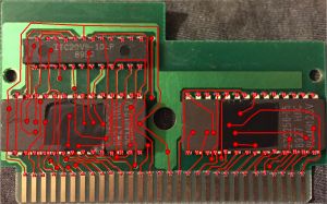
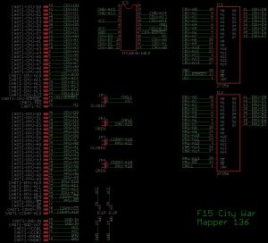
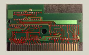
Here are PCB images of the original Idea-Tek release of F-15 City War, emulated as Mapper 173 according to the above description. Credit to MLX for opening his cartridge and taking the pictures.
That's a particularly persuasive job of deceptive marks on the IC. "20V8-10LP" strongly implies a specific programmable logic... but then pin 12 would have to be ground, and pins 2 and 3 would have to be inputs (and they instead go to CHR A13 and A14) pin 3 would have to be an input to be a PAL, and it instead goes to CHR A13.
You know what's really funny? I just sat down and tried to trace the pinout of that IC.
It's almost the same as the pinout of the 05-00002-010 ASIC:
pins 1-12:
??
CHR A15
CHR A13
??
+5
??
+5
Gnd
CPU D3
CPU D2
CPU D1
CPU D0
Pins 13-21 appear to be the same as on the mapper 36 page.
That's not quite what I see. I get:
Code:
Pin Meaning
1 Unconnected
2 Connects to a pad that can lead +5V or not; for this cartridge, the connection is not made. Must be a configuration pin of some sort.
3 CHR A13
4 Unconnected
5 +5V
6 Unconnected
7 Connected to Pin 5, +5V
8 PRG CE
9 CPU D3
10 CPU D2
11 CPU D1
12 CPU D0
13 CPU A0
14 CPU A1
15 CPU A8
16 M2
17 CPU ROMSEL
18 Cannot see where this is going.
19 GND
20 CPU A14
21 CPU A13
22 *maybe* CHR A14
23 Unconnected
24 Unconnected
Here is how far I came in my amateurish tracing attempt using crayons (so to speak).
If you want to take out your mapper 36 cartridge, you should find that a XOR value of FF should lower the "defective" pin 22, while a XOR value of 00 should raise it. If that is so, then Pin 22 is definitely CHR A14 on F-15 City War and Xiao Mali, otherwise I'm wrong.
NewRisingSun wrote:
2 Connects to a solder pad that can be +5V or not; for this cartridge, the connection is not made. Must be a configuration pin of some sort.
My bet is that that solderable jumper configures whether pin 1 of CHR ROM is connected to +5V or pin 2 of the ASIC.
Quote:
8 PRG CE
Definitely not. PRG pin 20 is grounded (look at the via on the far left side of F15CityWarBack). /ROMSEL must go to PRG pin 22.
Quote:
22 *maybe* CHR A14
I agree that topologically, CHR A14 could only go to 22 or 23.
Quote:
If you want to take out your mapper 36 cartridge, you should find that a XOR value of FF should lower the "defective" pin 22, while a XOR value of 00 should raise it.
Pin 22 was always high; various values written caused it to switch between "sourcing more current" and "sourcing less current" when directly connected to a white LED to ground.
Getting the test clips onto my cart again is enough of a pain I'd prefer to not do so again, but I believe it was accurate to say that much as pin 23 ultimately relayed values from pin 6, pin 22 (had it not been defective) would have relayed values from pin 8 (or maybe pin 9?).
Either way, based on the game's code, CHR A14 must be the inverse of the XOR value.
Quote:
My bet is that that solderable jumper configures whether pin 1 of CHR ROM is connected to +5V or pin 2 of the ASIC.
What would be the point of pulling pin 28 of the CHR chip low?
NewRisingSun wrote:
What would be the point of pulling pin 28 of the CHR chip low?
You're reading the solder jumper wrong:
Attachment:
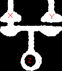 solder-jumper.png [ 573 Bytes | Viewed 4045 times ]
Depending on which pad is shorted, either X connects to Z, or Y connects to Z. (You don't short both and expect things to work afterwards)
On the F15 City War pictures you showed, "X" is +5V, "Y" is ASIC pin 2, and my hunch is that "Z" is pin 1 of the CHR, or A15.
Seems like I have to use my continuity meter? Can one point which pins specifically should be checked?
Pin 27 of the CHR chip (right chip, top row, second pin from left) should be connected to pin 22 or 23 of the ITC IC.
Well, I only got pin 8 wrong and gave up on pin 18, so I guess I did not do too badly for an amateur. Thanks, everyone. We also have the PCB images of
1991 賭馬 Racing (Enjoyable Horse Racing), Mapper 172. The bankswitching code is very similar, so the IC should be functionally similar, but comes in an 28-pin rather than a 24-pin package. But that's for another day (or week, or year).

lidnariq wrote:
pin 22 (had it not been defective) would have relayed values from pin 8 (or maybe pin 9?).
If anything, it would have to relay the
inverse of Pin 9 (D3), and while that one may work for
F15 City War and
Puzzle, at least as far as I have played, it certainly fails for 小瑪琍 (Xiǎo Mǎlí). The "inverse XOR value" story matches our results with the dumping script as well as the game code.
And since it was so much fun, here are PCB shots of Mapper 136 (Mahjong Trap) and Mapper 172 (1991 Duma Racing). These use a custom IC that is functionally similar to the beloved TXC 24-pin IC, except that it comes in an 28-pin package, having six instead of four CPU (data input) and data output pins. (Although if I understood lidnariq correctly, the 24-pin IC could have as many as six CPU pins connected as well, so I wonder which other four pins' function is missing.) Mapper 172 seems similar to Mapper 136 except that the custom IC is mounted upside down.
Mapper 136 (images from
Pepper-98):
Attachment:
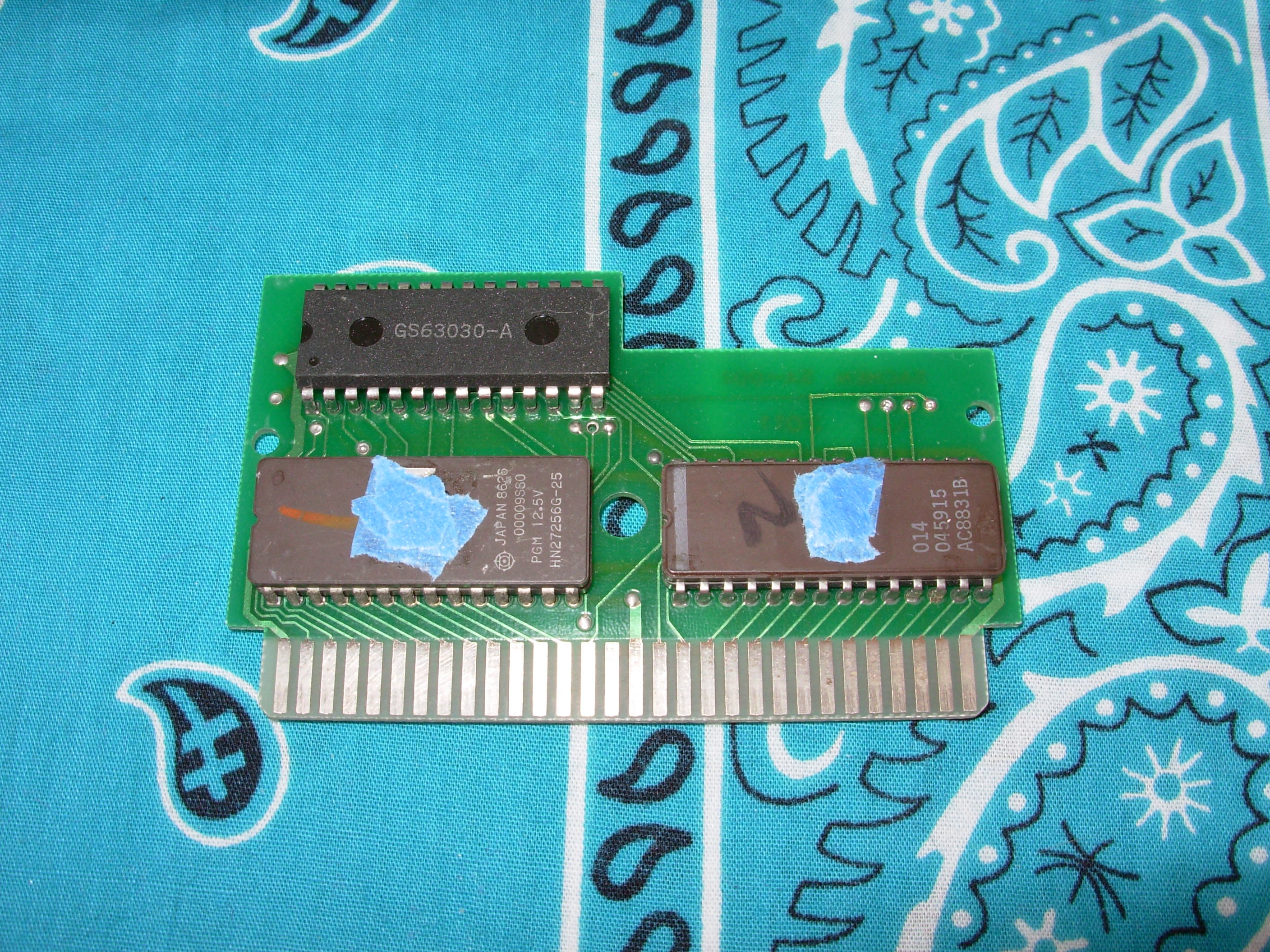 MahjongTrap-Front.jpg [ 1.28 MiB | Viewed 5097 times ]
Attachment:
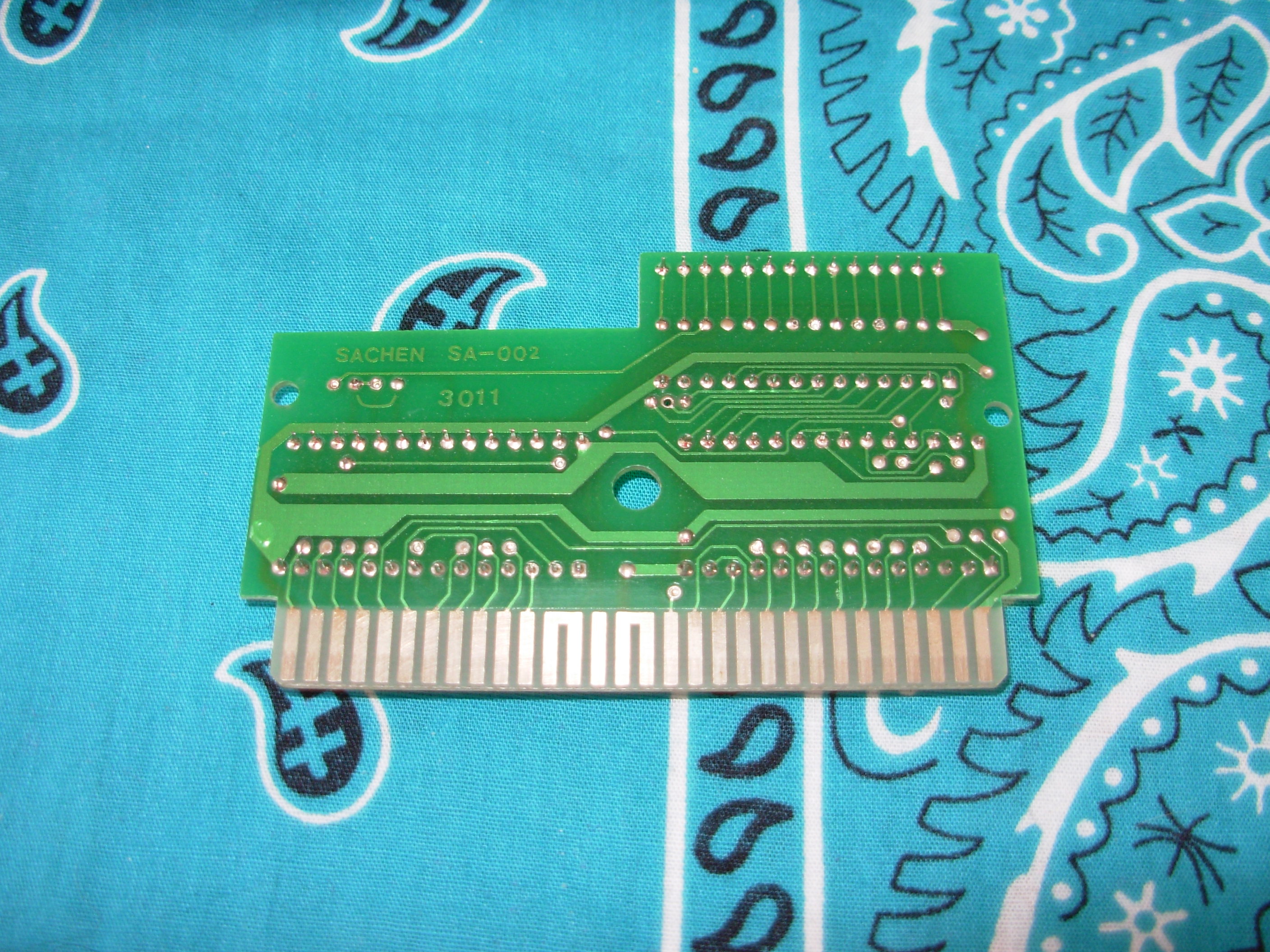 MahjongTrap-Back.jpg [ 1.29 MiB | Viewed 5097 times ]
Mapper 172 (images from MLX):
Attachment:
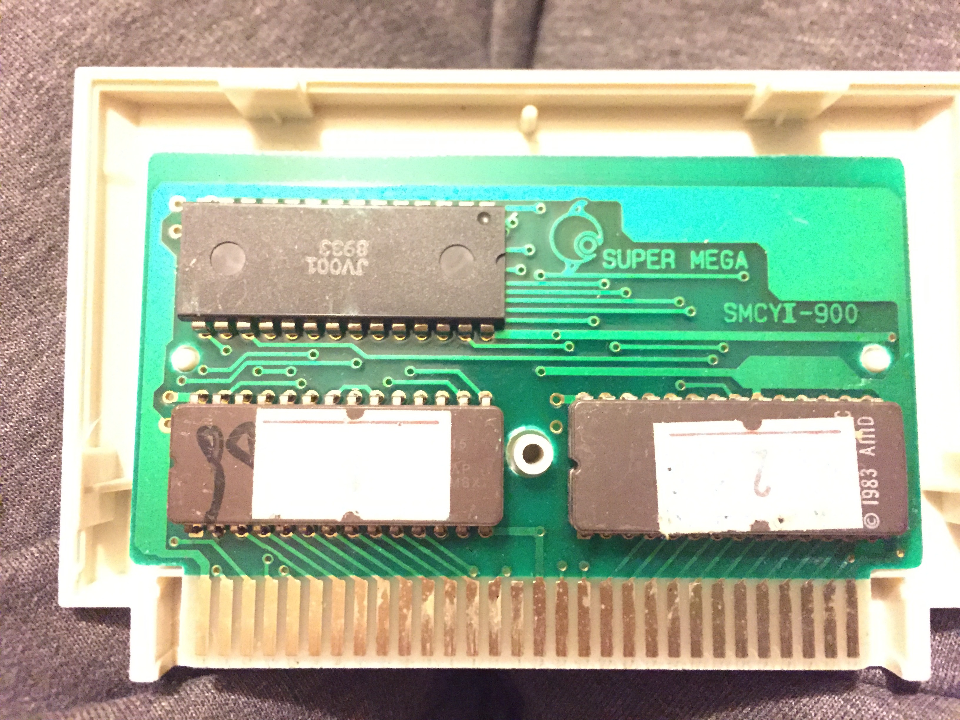 DumaFront.JPG [ 1.58 MiB | Viewed 5096 times ]
Attachment:
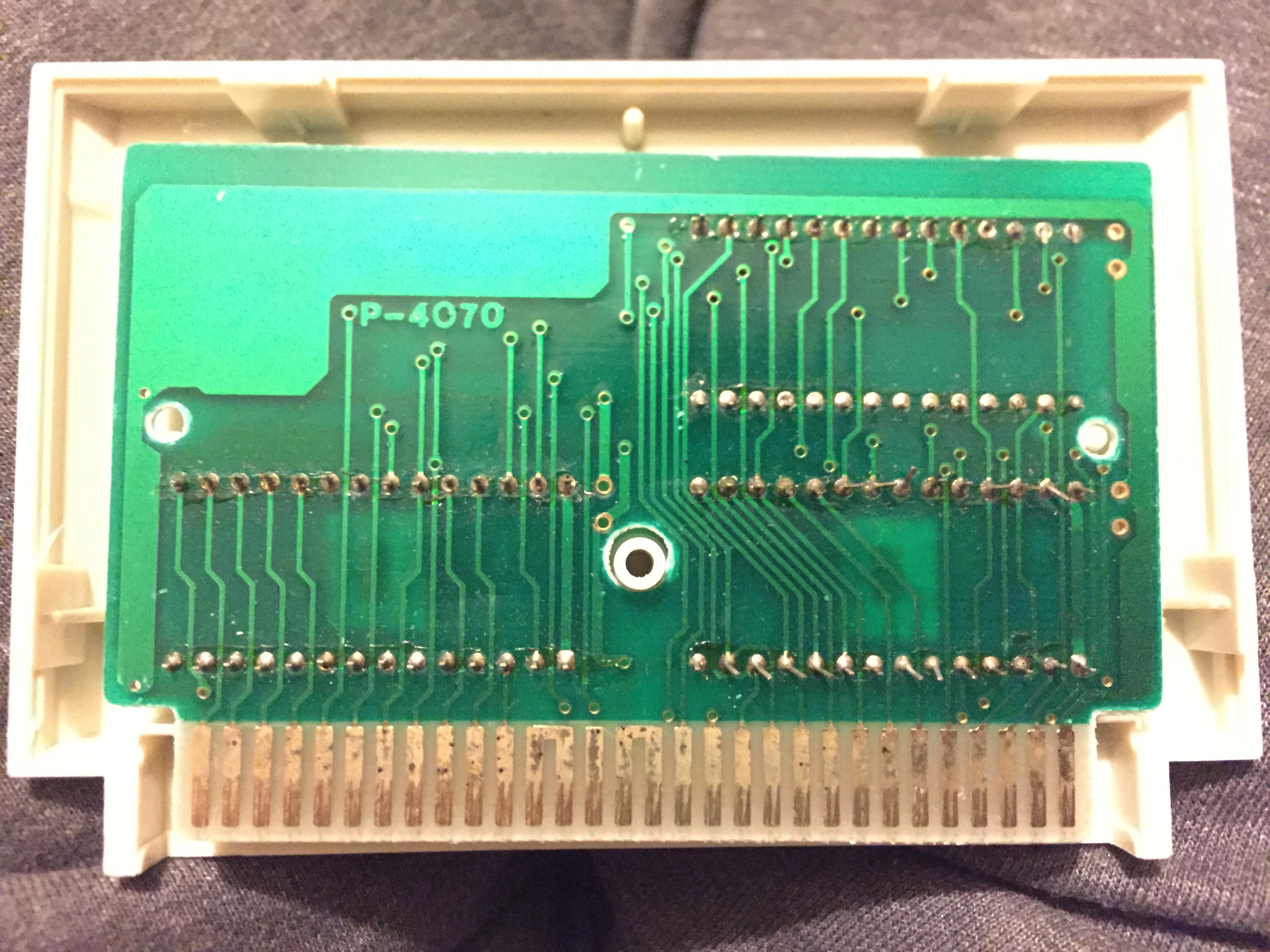 DumaBack.JPG [ 1.62 MiB | Viewed 5096 times ]
According to my trace attempt (correct me if I'm wrong), I identify the following JV001 pin functions:
Code:
Pin# Mapper 136 connection Mapper 172 connection General pin function
----------------------------------------------------------------------------
1 PPU A13 PPU A13 PA13
2 CPU D5 CPU D0 Input D5
3 CPU D4 CPU D1 Input D4
4 CPU D3 CPU D2 Input D3
5 CPU D2 CPU D3 Input D2
6 CPU D1 CPU D4 Input D1
7 CPU D0 CPU D5 Input D0
8 CPU A0 CPU A0 ($0001) A0
9 CPU A1 CPU A1 ($0002) A1
10 CPU A8 CPU A8 ($0100) A8
11 CPU M2 M2 M2
12 CPU /ROMSEL CPU /ROMSEL ($8000) /ROMSEL
13 CPU R/W CPU R/W R/W
14 +5V +5V +5V
15 CPU A14 ($4000) A14
16 CPU A13 ($2000) A13
17 CHR /OE CHR /OE CHR /OE
18 Output D5
19 Output D4
20 Output D3
21 Output D2
22 CHR A14 Output D1
23 CHR A13 Output D0
24 PPU A10 PA10
25 PPU A11 PA11
26 CIRAM A10 CIRAM A10
27 PPU R/W PPU R/W
28 GND/+5V GND/+5V
Which is odd, because that would mean that Mapper 172 has mapper-controlled mirroring, which nobody emulates. When MLX redumped Mahjong Block (Mapper 172 version), the Kazzo identified the mirroring type incorrectly, which would not happen in the case of fixed mirroring, so it's not entirely out of the question. I would not have any idea what write pattern selected the mirroring type though.
I found it easier to trace the Mapper 172 images, which is why the Mapper 136 column is rather empty. Yes, Mapper 172 has CPU D0..D5 connected in reverse, and the three Mapper 172 games indeed have code to reverse the desired six bits before they output the data to $4102.
@krzysiobal: I only noticed this now in your otherwise excellent schematic, but F-15 City War is Mapper 173, not 136. (The thread title was originally "Sachen TCU-2/Mapper 136" because that one started the thread. I have since renamed the thread title to reflect the expanded scope of the discussion.)
Mapper 147, original 60-pin version of the game (images from MLX):
Attachment:
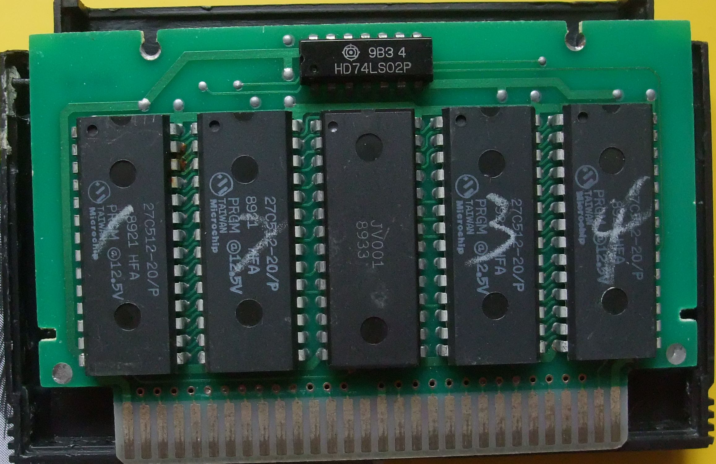 TC-011_fc_pcbf.jpg [ 473.9 KiB | Viewed 4913 times ]
Attachment:
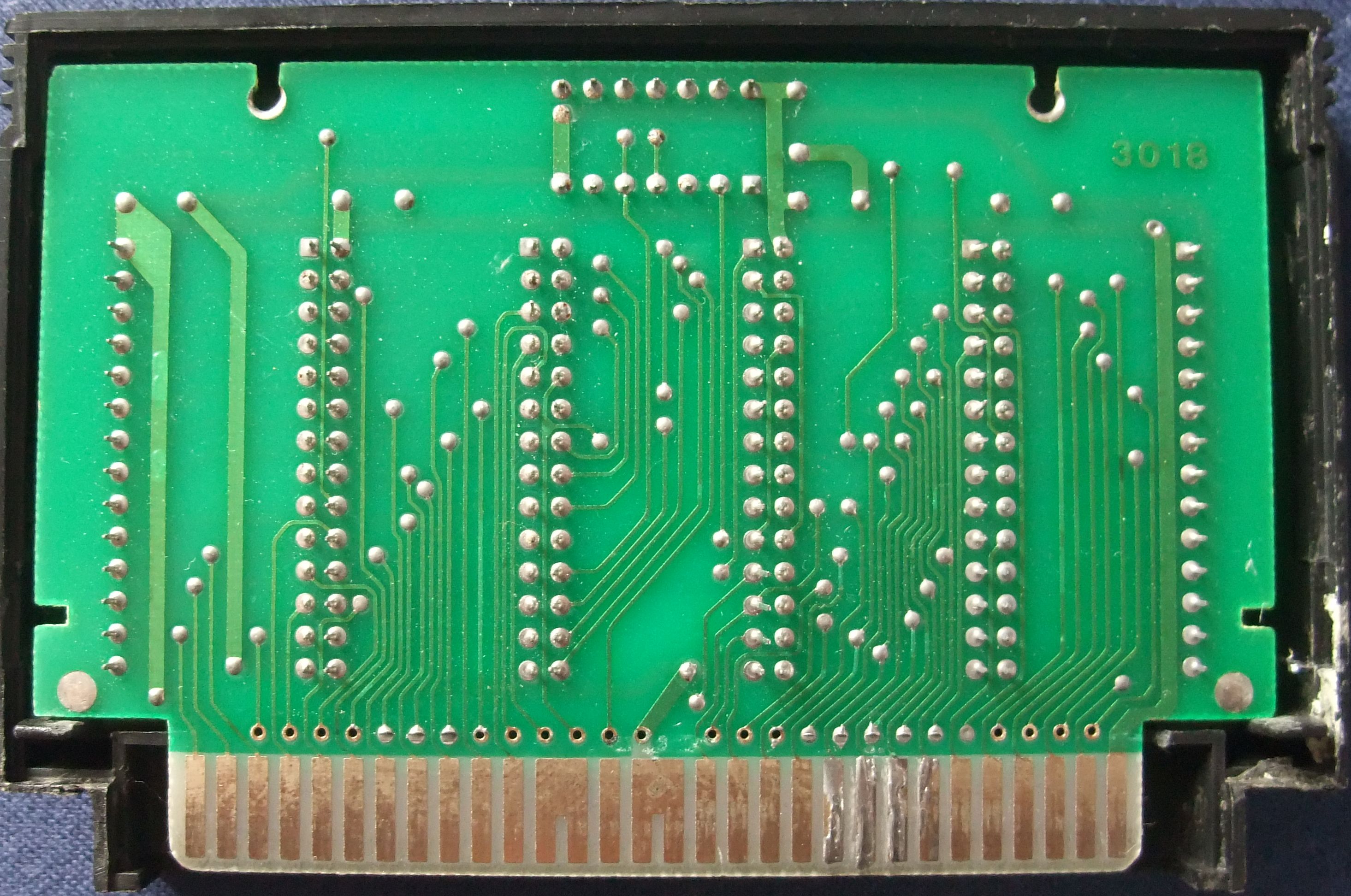 TC-011_fc_pcbb.jpg [ 815.84 KiB | Viewed 4913 times ]
And finally,
Mapper 132, to complete the TXC/Joy Van collection. Pictures again from MLX. Image from MGC-001 (Qiwang).
Attachment:
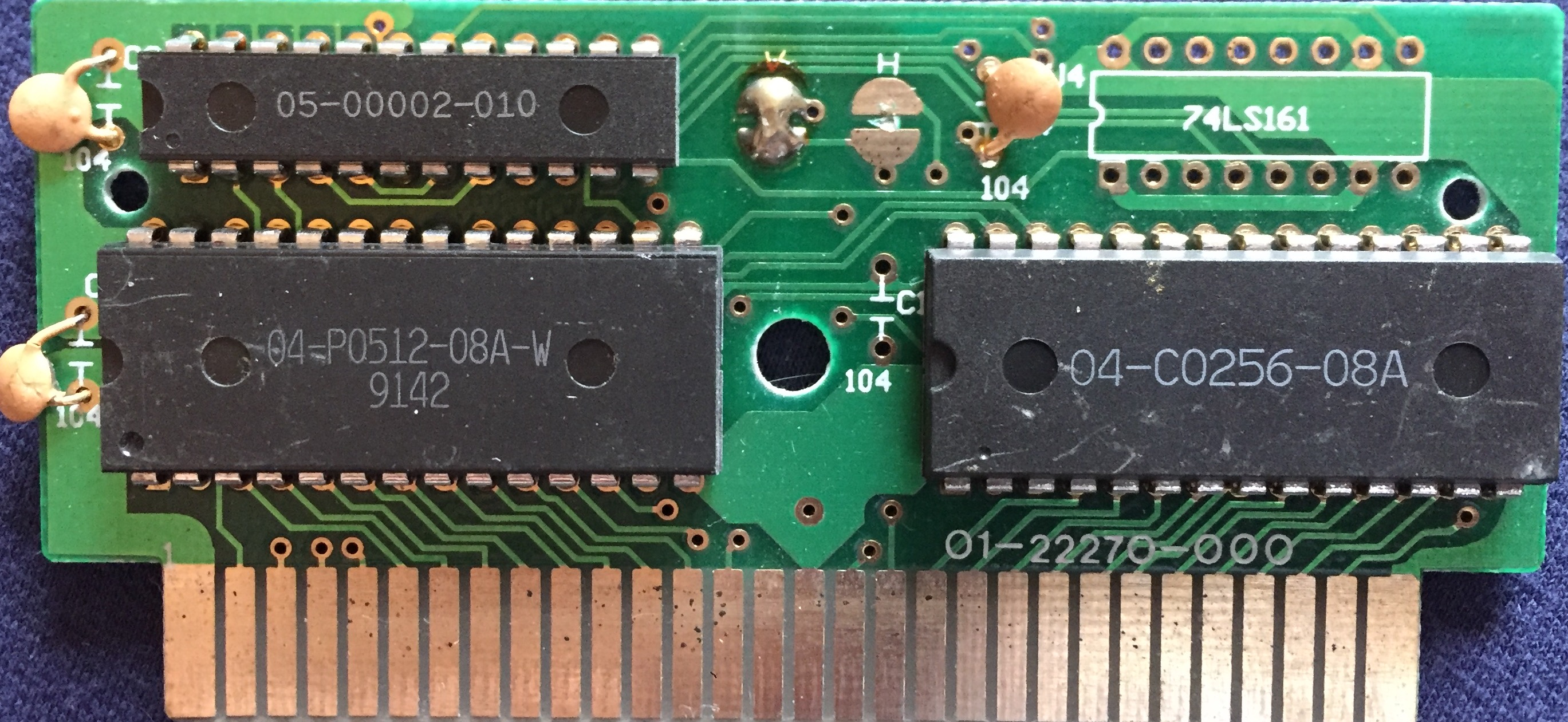 MGC-001 Front.JPG [ 937.97 KiB | Viewed 4898 times ]
Attachment:
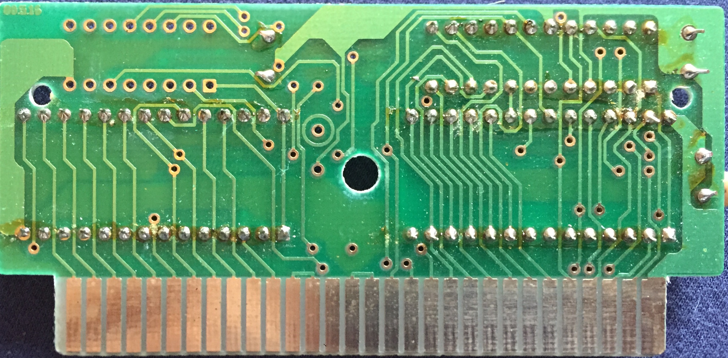 MGC-001 Back.JPG [ 1.05 MiB | Viewed 4898 times ]
Does somebody have an idea what the optional 74LS161 in that Mapper 132 board picture might be used for if it were installed?
Assuming it's a real 161... there aren't a lot of options for one by itself without extra hardware. Has to be present over the entire range from $8000-$FFFF, has to have bus conflicts, can't be anything finer than 32K PRG and/or 8K CHR.
Without tracing, I'd guess it's mapper 148.
(edit) ... Having now traced, I think too much information is hidden under ICs to be able to make a more informed guess. (edit2) It probably just latches the 3 LSBs of the data bus and uses them verbatim in some order as PRG A15, CHR A13, and CHRA14. Possibly the same order as mapper 133?
I can check your guesses with my continuity meter.
Fair enough...
Visibly true from the photographs:
'161 pins 1, 7, 10, 16 - tied to +5V
'161 pin 8 - tied to ground
'161 pins 11, 15 - floating
Almost guaranteed to be true:
'161 pin 2 - /ROMSEL - ASIC pin 17
'161 pin 9 - R/W - ASIC pin 18
Likely:
'161 pins 3-6 - CPU D0-D3 - ASIC pins 12-9
Necessarily true but but order unknown-
'161 pins 12-14 - PRG and CHR banking bits - ASIC pins 1,2,3,22,23? - PRG ROM pin 1, CHR ROM pin 26, 27
Guessing:
'161 pin 12 - ASIC 1 - PRG ROM pin 1
'161 pin 13 - ASIC 2 - CHR ROM pin 26
'161 pin 14 - ASIC 3 - CHR ROM pin 27
That reminds me: could you post images of your Mapper 036 board sometime please? I am close to identifying the function of all the 24-pin ASIC pins,
having done so for the 28-pin JV001 variant, but would like to take a look at that board as well first.
There are pictures in the dumping thread-
viewtopic.php?p=167180#p167180 - front
viewtopic.php?p=167183#p167183 - back
If you'd like nicer pictures I could put it on my scanner or something.
More pictures of component-side only of PCBs on
Gluk Video website; specifically "Puzzle", "F-15 City War", "Volley Ball", "Comando de Lobos", "Policeman".
Also has a picture of the 01-22003-400 PCB used by Creatom.
I am assuming that the 24-pin 01-22000-400 IC is functionally identical to the 28-pin JV001 IC except in pin count, and that the difference in pin count is solely due to the JV001 having six input and six output data bits, while the 01-22000-400 has only four input and four output data bits:
Code:
28-pin 24-pin Function (normative)
------ ------ --------------------
2 - Input D5
3 - Input D4
4 9 Input D3
5 10 Input D2
6 11 Input D1
7 12 Input D0
8 13 Input A0
9 14 Input A1
10 15 Input A8
11 16 M2
12 17 CPU /ROMSEL
13 18 CPU R/W
14 ? Vcc
15 20 CPU A14
16 21 CPU A13
17 ? CHR /OE
18 - Output D5
19 - Output D4
20 24 Output D3
21 1 Output D2
22 2 Output D1
23 3 Output D0
The JV001 also has a Mirroring control, using three pins: Input PA10, Input PA11, and Output CIRAM A10. PA10, PA11 are the inputs from the cartridge connector. $4101 D0 selects whether PA10 or PA11 is relayed to the JV001's CIRAM A10 output, effective once $8000-$FFFF is written to:
Code:
28-pin 24-pin Function (normative)
------ ------ --------------------
24 ? Input PA10
25 ? Input PA11
26 22 Output CIRAM A10
27 ? PPU R/W
28 ? GND
We know from the Mapper 173 analysis that the 01-22000-400 IC also has a pin that is similarly affected by $4101 D0: Pin 22, so it is most likely the CIRAM A10 equivalent. The question then is which pins are the equivalent input PA10 and PA11 pins. Unfortunately, no known board actually uses that IC for mirroring control, so we cannot observe that directly. But:
- On the Mapper 173 board, Pin 22 is connected to CHR A14. To deterministically be a 0 or 1 depending on $4101 D0, the Input PA10 pin must be connected to Vcc, and the Input PA11 pin must be connected to GND (or vice-versa).
- On the Mapper 036 board, Pin 22 is not connected to anything, but is reportedly always high but somewhat unstable depending on register values being written. This may be the result of a broken chip, as previously claimed, but I think it's the result of one of the two inputs being connected to Vcc, and the other floating but mostly picking up a high signal.
On Mapper 173, GND is on Pins 8 and 19 and VCC is on Pins 5 and 7. On Mapper 036, VCC is also on Pins 5 and 7, GND is Pin 19, while Pin 8 is not connected. I would suspect then that Pin 7 is Input PA10 and Pin 8 is Input PA11. Which means that if both were connected to GND, then Pin 22 should deterministically go Low after all.
After that, there are still three of the 24 pins with functions to distribute: Pins 4, 6 and 23. Of the JV001's functions, we still have PA13, CHR /OE, and PPU R/W. I'm not sure what the JV001 would need them for, but that's how they are connected on the Mapper 172 board.
Please note that my designations of D0-D5 are from the chip's point of view. Because the Mapper 172 board connects the CPU bits in reverse order, D5 is D0, D4 is D1 and so on, and Mapper 036's CPU D4/D5 are the chip's D0/D1.
lidnariq wrote:
'161 pins 1, 7, 10, 16 - tied to +5V
'161 pin 8 - tied to ground
'161 pins 11, 15 - floating
'161 pin 2 - /ROMSEL - ASIC pin 17
'161 pin 9 - R/W - ASIC pin 18
Correct.
lidnariq wrote:
'161 pins 3-6 - CPU D0-D3 - ASIC pins 12-9
D0 - 161.3 - ASIC.12
D1 - 161.4 - ASIC.11
D2 - ASIC.10 only
D3 - ASIC.9 only
161.5 - PRG.16
161.6 - PRG.17
lidnariq wrote:
'161 pin 12 - ASIC 1 - PRG ROM pin 1
'161 pin 13 - ASIC 2 - CHR ROM pin 26
'161 pin 14 - ASIC 3 - CHR ROM pin 27
161.12 - PRG.1 - ASIC.1
161.13 - CHR.27 - ASIC.2
161.14 - CHR.26 - ASIC.3
The 01-22111-100 PCB has the ASIC wired identically to the 01-22270-000 PCB, the only difference between the two is that the 01-22270-000 PCB has the spot for the 74LS161 while the 01-22111-100 PCB does not.
Comparing the 74LS161 pin functions to the ASIC pin functions as I find them, the 74LS161 at address $8000-$FFFF does exactly the same as the ASIC, only without the $4100-$4103 adder/inverter, which I understand basically as a protection method. I suppose that the 74LS161 configuration is then used for prototypes and development, while the ASIC configuration for production. The 74LS161 configuration would then have its data bits indeed like Mapper 133, but at $8000-$FFFF instead of $4100.
NewRisingSun wrote:
I am assuming that the 24-pin 01-22000-400 IC is functionally identical to the 28-pin JV001 IC except in pin count, and that the difference in pin count is solely due to the JV001 having six input and six output data bits, while the 01-22000-400 has only four input and four output data bits:
But I know that to be untrue?
There are six data bus pins on the 05-00002-010 IC, divided into two functional groups of three.
Pin 24 on the 05-00002-010 is unequivocally carry-out from the bits latched into pins 12-10 and exported on pins 3-1.
Quote:
On the Mapper 036 board, Pin 22 is not connected to anything, but is reportedly always high but somewhat unstable depending on register values being written. This may be the result of a broken chip, as previously claimed, but I think it's the result of one of the two inputs being connected to Vcc, and the other floating but mostly picking up a high signal.
I mean, it unequivocally can switch between two different amounts of current sourced when pulling up. I don't see an obvious way for that to happen short that either being deliberately designed in (but I have no idea why), or damage to the IC.
lidnariq wrote:
Pin 24 on the 05-00002-010 is unequivocally carry-out from the bits latched into pins 12-10 and exported on pins 3-1.
That's what I said: Input bit 0 (pin 12), Input bit 1(pin 11) and Input bit 2 (pin 10) relayed to Output bit 0 (3), Output bit 1 (2) and Output bit 2 (1), and Input bit 3 (9) relayed to Output bit 3 (24). But have you checked, or are you just assuming based on what looks like functional groups, that a fifth and sixth bit are indeed directly relayed as well? Right now, the Mapper 036 article says that if Pin 22 weren't defective, you assume it would relay some other pin, but that's just conjecture and directly contradicted by Mapper 173's connection.
Edit: No, actually it doesn't say that. It says that Pin 22 is always defective, and Pins 23 and 24 relay something else, although I am note quite sure what.
lidnariq wrote:
I mean, it unequivocally can switch between two different amounts of current sourced when pulling up.
With the inputs that two other pins have, yes. What I am proposing is that if certain other pins (possibly 7 and 8, but I am not sure about that yet) were not connected as they are on the Mapper 36 board, but as they are e.g. on the Mapper 173 board, things would be different, and you would observe normal high and low states.
NewRisingSun wrote:
Input bit 3 (9) relayed to Output bit 3 (24). But have you checked,
I am confident that pin 9 is not relayed to pin 24, even though this contradicts what you've found on other ICs with the same marking.
Quote:
or are you just assuming based on what looks like functional groups, that a fifth and sixth bit are indeed directly relayed as well?
Pin 6 was definitely relayed to pin 23.
Pin 6, 8, and 9 in that order obeyed increment behavior when set to increment mode and reading back from the register inside, separate from pins 12, 11, and 10 in that order.
I'd want a less cranky test system than my current hot-swappable thing if I'm going to do more testing.
Quote:
What I am proposing is that if certain other pins (possibly 7 and 8, but I am not sure yet) were not connected as they are on the Mapper 36 board, but as they are e.g. on the Mapper 173 board, things would be different, and you would observe normal high and low states.
I'm going to have to desolder this, aren't I...
No, don't desolder anything just for me.

The original question was what the 74LS161 spot was for, and that was answered thanks to MLX' testing, so let's leave it at that for now.
I think the current pinout should be rewritten though to clearly state which pin is relayed to which, instead of how the pins are connected on that particular board, as the current description is giving me a headache.
MLX wrote:
D0 - 161.3 - ASIC.12
D1 - 161.4 - ASIC.11
D2 - ASIC.10 only
D3 - ASIC.9 only
161.5 - PRG.16
161.6 - PRG.17
[...]
161.12 - PRG.1 - ASIC.1
161.13 - CHR.27 - ASIC.2
161.14 - CHR.26 - ASIC.3
.... fascinating. That's latching D0, D1, D4, and D5. Looks like ... GNROM? Yeah, specifically MHROM.
Ah, now it's becoming clear that 6, 8 and 9 are connected in reverse order from 10, 11 and 12. Now the increment can work on both triples without breaking the Mapper 173 games. The $4101 part still needs to be added to the Mapper 036 page (or better yet, the IC's page). Was it that Invert is applied to the 10/11/12 tuple when writing to $4100 and Mode=0, and to the 6/8/9 tuple when reading from $4100?
Invert appeared to be applied on a bit-by-bit basis (i.e. "XOR") when I did testing last time -
viewtopic.php?p=196783#p196783
Unfortunately, that will not work with Puzzle, which writes $01 to $4101 yet expects all bits to be inverted. That, and the mystery pin 22 still need to be investigated, and since all Mapper 173 games explicitly vary their $4101 value between 00 and FF to select CHR A14, which is connected to Pin 22, the two must *somehow* be connected, possibly with the help of another pin.
Given that mapper 173 flows data from pins 12, 11, 10 to, in order, pins 3, 22, 2 ... I have to wonder if it's actually the same part or just close enough to be trolling us.
No, 11 explicitly doesn't flow to 22. That's the whole point of Xiao Mali's protection. Like I said, CHR A14 only comes from the $4101 value, not from anything ever written to $4102.
Oh... somehow I'd gotten confused.
Per your description of mapper 173, on my mapper 36 board, shouldn't writes to $4101 have done something to the resultant bank?
e.g. the sequence
$00 -> [$4103]
$30 -> [$4102]
$30 -> [$4101]
xx -> [$4100]
xx -> [$8000]
should cause bank 0 to be mapped, and also 0 to read back from the ASIC?
In contrast, writing 0 to $4101 should have caused bank 3 to be mapped and 3 to read back from the ASIC?
I'm pretty certain that writes to $4101 had just no effect at all when I was testing before, but if it doesn't involve test clips I'm willing to play with hot-swapping things again.
No, because Mapper 36 does not connect Pin 22 to any PRG or CHR pins, but Mapper 173 does, and I'm still insisting that Pin 22 is operated by $4101. Basically, the way I think it works (and the only way that emulation works) is like this: Writing anything to $8000-$FFFF not only copies the internal register bits (originally from pins 6/8-12) to the output pins (1-3, 23, 24), but also copies the inverse of the $4101 state to Pin 22. Note that I do not expect that writing to $4101 alone without being followed by the usual $4103/$4101/$8000 sequence will have any effect. Because Pin 22 is not connected to anything on Mapper 36, you will not be able to see the effect from hot-plugging alone without connecting something, either a LED or a voltmeter, to Pin 22.
To get 8 KiB CHR bank 0 in Mapper 173, you must write: $FF to $4101 and $x1 (AND $01) to $4102 (and then the usual rest).
To get 8 KiB CHR bank 1 in Mapper 173, you must write: $FF to $4101 and $x0 (AND $01) to $4102 (and then the usual rest).
To get 8 KiB CHR bank 2 in Mapper 173, you must write: $00 to $4101 and $x0 (AND $01) to $4102 (and then the usual rest).
To get 8 KiB CHR bank 3 in Mapper 173, you must write: $00 to $4101 and $x1 (AND $01) to $4102 (and then the usual rest).
The other bits in $4102 are only relevant for the game reading back from $4100 and checking its value. You can see it yourself in the Mapper 173 dump of
Puzzle from PC $E6F5 on (which also does three increments, so it'll be a bit more complicated). Here's the equivalent Kazzo script, also with three increments since it was just copied after the game's code:
Code:
function ppu_dump(d, pagesize, banksize)
{
for(local i = 0; i < pagesize; i++){
local xorvalue = ((i >> 1) & 1) * 0xFF) ^ 0xFF;
cpu_write(d, 0x4101, xorvalue);
local written = (((i & 7) - 3) & 7) | (i & 8);
cpu_write(d, 0x4102, written ^ xorvalue);
cpu_write(d, 0x4103, 0);
cpu_write(d, 0x4100, 0);
cpu_write(d, 0x4103, 0xFF);
cpu_write(d, 0x4100, 0xFF);
cpu_write(d, 0x4100, 0xFF);
cpu_write(d, 0x4100, 0xFF);
cpu_write(d, 0x80EF, 0xFF);
ppu_read(d, 0, banksize);
}
}
Sure? I wasn't talking about the CHR A14 bit on mapper 173, but rather what's going on with the readback value.
For mapper 173, you wrote
Code:
Read $4100-$4103: [.... RRRR]: Read Register. Bit 3 is inverted if Invert==1. Bits 4-7 are open bus.
Write $4100: When Mode==0: Bits 0-3 of Register := Input, bits 0-2 being inverted if Invert==1.
When Mode==1: Bits 0-2 of Register incremented by one, bit 3 unaffected.
Write $4101: Invert := Written value bit 0.
Write $4102: Input := Written value bits 0-3.
Write $4103: Mode := Written value bit 0.
Write $8000-$FFFF: Output := Register; written value is ignored.
so if I write 0 to $4103, then 0 to $4102, then $10 to $4101, and then anything to $4100 ... the value I read back from $4100 should be something other than 0, right? Or am I confused?
All games always write to $4101 before writing to $4102, and then do not write to $4101 until they have read from $4100 to check its result. So honestly I have no idea what to expect when writing to $4101 after you have written to $4102. That will have to be investigated.
I do think that we should investigate the $4101->Pin 22 issue first (assuming you don't insist on the "broken chip" explanation).
I have a ET.02 Xiao Ma Li up for grabs. So if any of you want it to have some fun with the ITC20V8…
NewRisingSun wrote:
All games always write to $4101 before writing to $4102, and then do not write to $4101 until they have read from $4100 to check its result. So honestly I have no idea what to expect when writing to $4101 after you have written to $4102. That will have to be investigated.
What I'm trying to get at isn't the order, but instead that it seems that writes to $4101should have done anything at all on mapper 36, unless I'm really misunderstanding things.
Quote:
I do think that we should investigate the $4101->Pin 22 issue first (assuming you don't insist on the "broken chip" explanation).
I can't rule out that behavior having something to do with pins 4-8 being wired differently.
MLX wrote:
I have a ET.02 Xiao Ma Li up for grabs. So if any of you want it to have some fun with the ITC20V8…
I unfortunately only have a front-loading NES and no famicom-to-NES adapter, so would have difficulty doing any tests.
(short of desoldering it)
Quote:
What I'm trying to get at isn't the order, but instead that it seems that writes to $4101 should have done anything at all on mapper 36, unless I'm really misunderstanding things.
Let me revise what I have previously written to more accurately answer your question. The snipped you quoted, if correct, would say in terms of chip pins (and with my new understanding that there are really six bits plus one carry bit, even if Mapper 173 only connects four of them):
- Writing to $4101 changes Invert to Pin 12's value.
- When $4100 is written to and Mode is 0, the value previously written to $4102, being the triplet from Pin 10-12 and the triplet from Pin 6/8/9, is copied into Register. If Invert is active, the triplet from Pin 10-12 is inverted during copying, while the triplet from Pin 6/8/9 is not inverted.
- When $4100 is read from, the two triplets from Register are copied to Pin 6/8/9 and Pin 10-12. If Invert is active, the triplet copied to Pin 6/8/9 is inverted during copying while the triplet copied to Pin 10-12 is not inverted.
- When $8000 is written to, Register is copied to Output, and Pin 22 goes high if Invert is inactive and low if Invert is active.
The basic hypthesis here is that $4101 inverts one triplet during writing only and the other triplet during reading only.
On Mapper 36, since only two bits of the Pin 10-12 triplet and none of the bits of the Pin 6/8/9 triplet are connected, writing a value to $4102+$4100 with Invert
inactive, then activating Invert, then reading via $4100 will return the same value because reading $4100 only inverts the non-connected triplet. Writing a value to $4102+$4100 with Invert
active and reading it back via $4100 should however invert it. This is something you can test without clips.
Ok, great, my earlier analysis was wrong. Writes to $4101 do have an effect.
If I specifically write:
$30 → [$4102]
$10 → [$4101]
xx → [$4100]
then the value read back is $4F (D7, D6, D3-D0 open bus)
If I write
$30 → [$4102]
$20 → [$4101]
xx → [$4100]
then the value read back is $7F.
Subsequently, if I just write
$10 or $00 → [$4101]
xx → [$4100]
then the value switches to $4F and $7F as appropriate.
My hotswap test reads back after every write, and the value read back doesn't change until the final write to $4100.
Yes, that seems compatible with my description. I have further edited it to highlight the importance of the final $4100 write. The experiment also nicely shows that only Pin 12 is relevant during the $4101 write. As for $4101 inverting the 6/8/9 triplet while reading from $4100, as I hypothesized, you will not be able to test this with a Mapper 36 board without using clips, as these pins are not connected to the CPU data bus.
Mostly I was just worried about my earlier (incomplete) evidence implying a difference between your required behavior in mapper 173 and what I'd observed in mapper 36. But now that's resolved cleanly.
MLX wrote:
I have a ET.02 Xiao Ma Li up for grabs. So if any of you want it to have some fun with the ITC20V8…
Oh, actually. There's a few simple tests that would let us determine whether pin 4 is an input/output or connected internally to the other ground pin. Would you be willing to do them?
They're:
* measure resistance between pin 4 and pin 19 — whether it's more or less than a couple kiloohms
* measure diode drop across pin 19 to pin 4 — whether it exists
* measure diode drop across pin 4 to pin 5/7 — whether it exists
Alright. My multimeter is kinda primitive so I'm not sure it's going to meet your expectations.
1-2) I can't, pin 4 is grounded by a trace under the IC (from pin 19).
3) Since the multimeter only has ohmic and continuity functionnality, I can't mesure any voltage drop… but we can still check both side:
4->5, 4->7: 520 Ohm
5->4, 7->4: 637 Ohm
The same value were observed for both 5 and 7.
Since it's straight grounded.
MLX wrote:
1-2) I can't, pin 4 is grounded by a trace under the IC (from pin 19).
Argh. Well, ok, that's the answer we're going to get for that question.
My hypothesis is still that Pin 4 was meant to take PA10 as an input and Pin 5 was originally meant to take PA11, and Pin 22 meant to output to CIRAM A10, relaying Pin 5 if $4101 D0==0 and Pin 4 if $4101 D0==1, just as Pins 24/25/26 on the JV001 ASIC. With Mapper 173 tying Pin 4 to GND and Pin 5 to Vcc, under this hypothesis, Pin 22 would instead constantly output 0 or 1 depending on the $4101 setting.
I realized that I could easily use a wire-wrap tool to non-destructively add connections to my copy of Policeman ... if we can think of any tests where that would be useful.
Unfortunately, I don't see an easy way to read back the contents of pins 1,2, and 24-22 without adding a lot of extra hardware.
Testing the functions of Pins 4, 5 and 22
Test 1: Connect a LED to Pin 22. Do the $4101/$4100 write sequence (#1: $4102=$30, $4101=$10, $4100=xx. #2: $4102=$30, $4101=$20, $4100=xx) and see if the LED changes.
Test 2: Swap the connections of Pins 4 and 5 from GND/Vcc to Vcc/GND and see if the way the LED change is now reversed. (I'm not sure if this can be done with wire-wrap?)
I think you wrote that you connected a LED to Pin 22 before, but as I understand your posts, you had not done the $4101 write sequence correctly before.
@MLX: Can you check on a Mapper 173 board (Xiao Mali or F-15 City War) if Pin 6 is indeed unconnected or connected underneath the ITC IC to some other pin (possibly also Pin 19)?
NewRisingSun wrote:
Test 1: Connect a LED to Pin 22. Do the $4101/$4100 write sequence (#1: $4102=$30, $4101=$10, $4100=xx. #2: $4102=$30, $4101=$20, $4100=xx) and see if the LED changes.
Bright side: Your hypothesis is at least mostly correct; pin 22 is definitely ... at least approximately ... a latched copy of pin 12 on writes to $4101. It changes immediately on writes to $4101; no need to write to any other register.
Down side: Pin 22 on my IC emits a variety of different high frequency signals.
My initial test consisted of four "old" LEDs, connected in series, from +5V to ground. None light. I then connect the middle leg (two LEDs both above and below) to the pin and ... somehow all four LEDs light up in different brightnesses.
Well, that's odd. Oscilloscope time!
... That's worse. Pin 22 is some logical function of other pins, depending on what value was latched to $w4101/pin12. I spent some time comparing it to other pins and it wasn't obviously the same as anything else. It is more-or-less synchronous, however.
... I tentatively think, that when the value written to pin 12 is 0, the resulting signal is pin 6 OR pin 8.
... and that when the value latched is 1, the resulting signal is just pin 8?
Using wire wrap, I'd connected CPU D0-D2,D6 to pins 6, 8, 9, 10 as I specified in the pinout—the code in Policeman doesn't care.
Pins 8 and 9 (what I've connected to D1 and D2) is definitely unequivocally latched via $4102 and can be read back immediately. Pin 6 isn't latched on writes to $4102—instead it seems that 0 is always latched, but the value read back is inverted according to the invert bit in $4101. (In other words, pin 6 reads back the inverted value latched into pin 12)
... and I realize now that I completely forgot to play around with what writes to $4103 did, if anything, to any of the above.
Quote:
Test 2: Swap the connections of Pins 4 and 5 from GND/Vcc to Vcc/GND and see if the way the LED change is now reversed. (I'm not sure if this can be done with wire-wrap?)
That definitely requires desoldering.
Also, just in case anyone else is tempted: DON'T do this before making sure that pins 4 and 5 are not internally connected to pins 7 and 19. If you connect 5V across the bond wires and a silicon trace inside that'll assuredly blow something up.
Pin 6 is totally unconected. Also if I put the positive electrode on pin 6 only 7, 8 (=19) give some continuity result while most will if pin 6 is negative.
lidnariq wrote:
That definitely requires desoldering.
Would you be willing to do such a thing and run tests if I purchase the offered Xiao Mali cartridge from MLX and reimburse him for shipping it to you?
Economy shipping (2 weeks to 1 month) is cheap. I don't mind paying that. But if you want to get it in 10 days, that's different.
Yeah, sure, I'm willing to desolder a chip and set up a less cranky testbed. I'm in no rush.

