Hi guys,
I recently got it into my head that I'd like to learn how to make some custom carts. I bought a Willem programmer, and flashed some homebrew stuff onto some w27c512's and swapped them onto a NES donor board and it worked no problem. Too easy. Now I want to learn something a little more advanced and I'd like to do so on the Game Boy. I was hoping someone could give me a few pointers along the way.
I want to set up a prototyping board for the Game Boy Color and I just cannot get it to work. I've been basically following the guide located here:
http://tinyurl.com/a78hsshThe cart I'm using for a donor is "Millennium Winter Sports" and it's a DMG-A06-01 board, just like the board in the guide. I desoldered rom from the board, and spent a couple hours carefully splicing together some jumper wires with some 30 AWG and then soldering them to the board. I wired up an AT49F040A-55JI PLCC in a PLCC32 to DIP32 Adapter board. After a couple hours of tinkering I'm at a loss as to why it's not working. The chip flashes and verifies just fine. I checked continuity between the pins of the PLCC socket and where they should route to on the cartridge connector and cant find any shorts.
The only thing I can think of is maybe there is an issue with my adapter board. There are some diodes on the board that I even tried shorting to see if they were interfering but no luck. My rom file should be ok as far as I can tell. I double it up to 2MB, and looking at the header I can see where the Nintendo logo is stored at 104h.
I've attached a couple photos of what I have going on. Probably not the easiest to make out but should give you some idea of where I'm at. At this point I'm about ready to pull it all apart and start with a new board.
Actually I'd like to make a second board, with an MBC1 donor board. Hopefully that'll be a bit simpler. I'd like to use a w27c512 for that but it's 28 pins and I'm not sure what to do with the extra unused pins on the board.
Any input on where I might be going wrong would be greatly appreciated.
Thanks guys!
Attachment:
File comment: Rom header
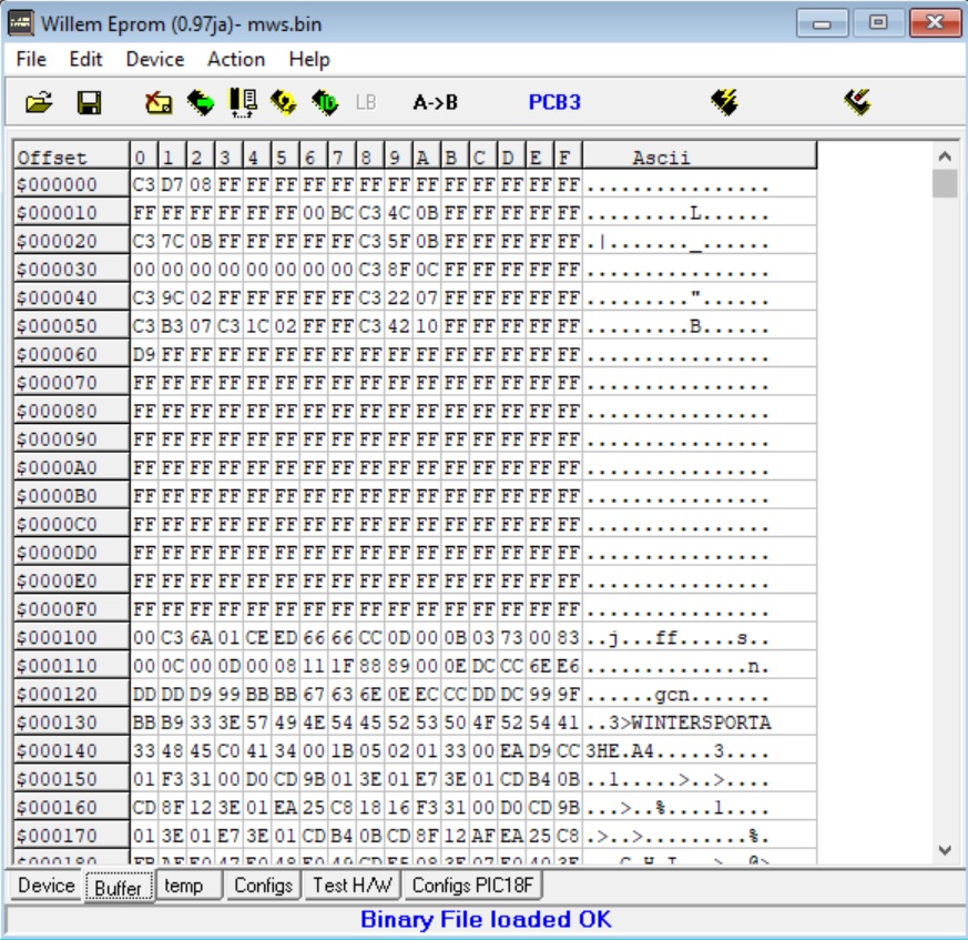 rom header.jpg [ 332.91 KiB | Viewed 5778 times ]
Attachment:
File comment: Board
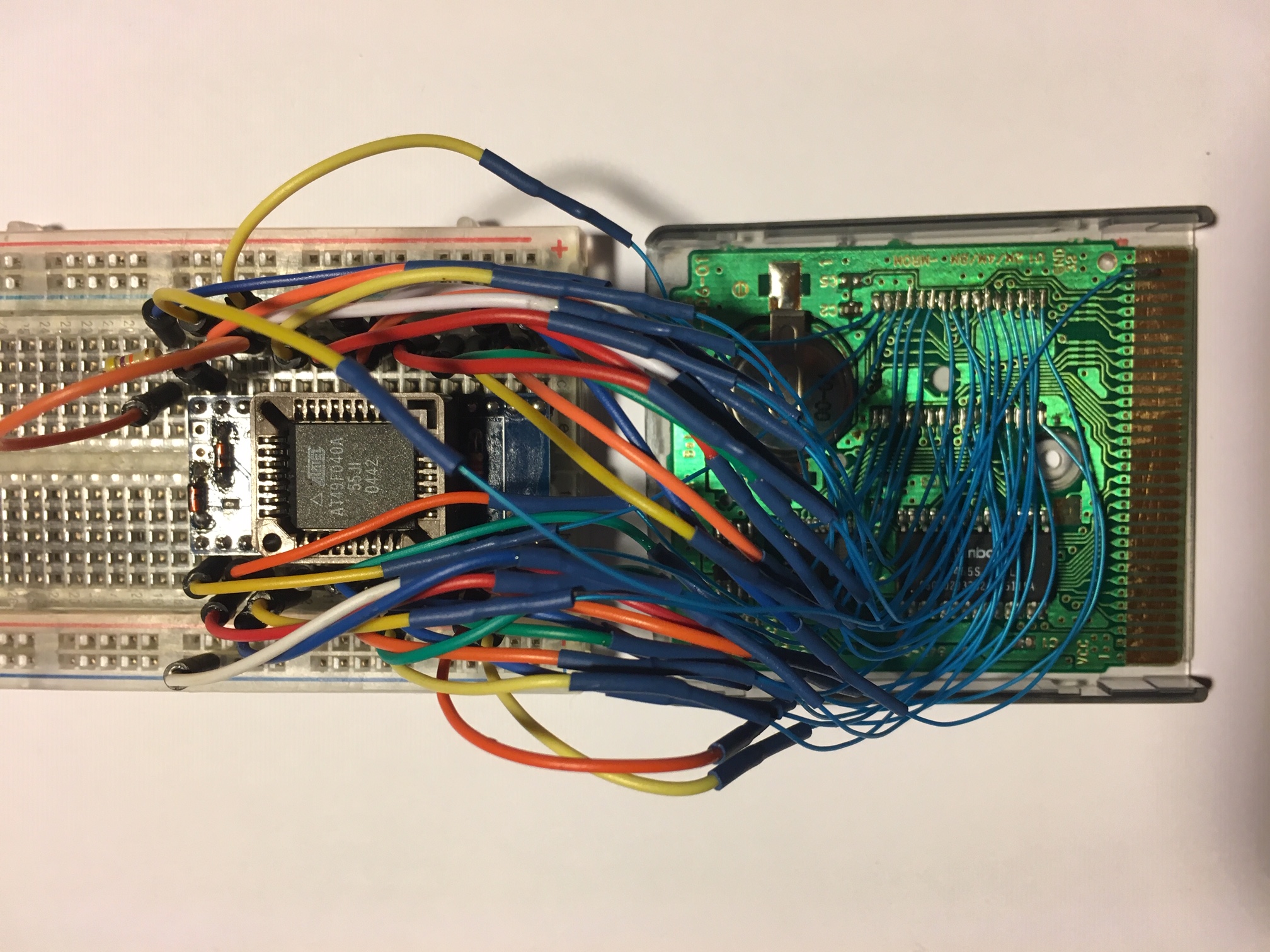 IMG_1071.JPG [ 871.92 KiB | Viewed 5778 times ]
Why did you solder a wire to DMG pin 31?
The diodes were there just for battery-backed RAM for save games... they shouldn't be related to the ROM at all.
The wire soldered to pin 31 is for programming with a GB Cart flasher. It's not needed but I figured why the heck not.
And I didn't mean the diodes on the donor board, there's a couple diodes on that PLCC to DIP converter I'm using.
I don't obviously see anything wrong with the abstract concept of your wiring... obviously it's sufficiently spaghetti that it's hard to figure out if any given thing is right.
What do the adapter board diodes do? It looks like they're a diode OR of some sort?
Where'd you get that breakout?
I'm assuming they're just some sort of bias protection. The breakout came with my willem programmer. It's actually this one here:
http://www.sivava.com/index.php?route=p ... uct_id=147
Uh... man, I can't see anything useful in that picture. At least one other picture I found of something similar looking replaces one of the diodes with a two-pin header and jumper.
The AT49F040A uses all 32 of its pins uniquely; so you'll need access to all 32 of them when you're using it on the cart. Whatever the diodes are doing, they somehow reduce the number of pins in a way that I suspect is getting in your way. Given their location, it looks like it's somehow routing PGM or WR from either pin 1 or pin 31, but for the game boy to work, you'll need to make sure that the AT49F040A /WR pin stays high during normal operation, and that A18 comes unimpeded from the MBC.
So I desoldered the diodes and fiddled around some more. Flashed a different rom to the chip and tried that. Still no luck...
Is pin 31 where the rom chip goes actually A18? In the guide I'm following it's listed as Vcc but I looked up the pinout of the MBC5 and it seems to be routed to A18.
Yeah, I'd expect in a Mask ROM that A18 would be pin 31, while on flash it's pin 1.
What should I do with OE1? Can I just leave it floating?
What OE1? Neither the flash chip nor the MBC5 have a pin by that name...
Generally unneeded outputs should be ignored.
What's the top left corner here? First pin
This is basically what I'm following:
Attachment:
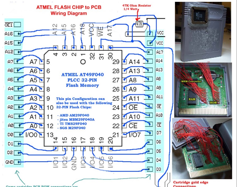 board diag.jpg [ 257.61 KiB | Viewed 5711 times ]
I have no idea. You'll have to use a continuity meter to figure out what the adapter board is doing, and then change things to accommodate that. I would help more if I could, but I literally cannot see what the traces are doing on the adapter board, and so cannot tell you what you have to change.
I do suspect that everything except the connections to the adapter pins 1 and 31 are fine. I expect those two pins are wrong.
The AT49F040A itself has no OE1 pin.
As stated in your image with a 47kΩ pullup, if you connected AT49F040A /WR (pin 31) directly to the card edge pin 31 (Audio) without a pull-up, you'll need to add a pull-up. The pin will float, probably to ground, and the flash part will only work as a ROM if /WR is high. Your initial picture doesn't obviously have a jumper to the other end of the resistor in your protoboard.
Yeah, I don't think I'll be able to get a clear shot of everything. I appreciate you trying to help. I'm gonna disconnect everything, wire it all up again and if that still doesn't work i'm going to try with a new board. Maybe I toasted something while tinkering around.
Is it possible to wire up a 28pin dip to one of these boards? What would I do with the missing 4 connections?
Well, you're only going to fit 64 KiB games in a 28-pin 'PROM, but you could put one on. As ever, ignore extra outputs from the MBC, and make sure all pins on the ROM actually are connected.
I do think you're giving up a bit prematurely, but you do have to figure out what the adapter board is doing to be able to make the AT49F040 work.
Ok so I ordered a new PLCC->DIP adapter board and that solved my problem completely. The pinout of the new board is exactly the same so as far as I can tell one or more of the pins on the old board aren't making good contact. So now with the little rig I made I've been able to successfully load from both an AT49F040A and a W27C512.
Now I've been working on building a new adapter that doesn't use a memory mapper at all. It basically breaks out the edge connector to a 34pin IDC cable. For the 2 extra pins I've doubled up on Vcc and GND's. To make things easy I've wired the connector to match the pinout of the W27C512. As far as I can tell I should be able to load a 64KB game off a W27C512 without issue. Again I am having issues getting anything to boot. I have it wired as follows:
A0-A15 -> A0-A15 (obviously)
D0-D7 -> Q0-Q7 (obviously)
OE -> RD (Pin 4 of edge connector)
CE -> CS (Pin 5 of edge connector)
I'm not sure if this is correct. I've checked continuity between everything and everything seems to be routed correctly. Also weird shorts between anything. I checked resistance between the pin connector on the gameboy and the eprom pins and found a couple bad jumper cables so I replaced them. I'm not sure if I need any capacitors or resistors in this circuit anywhere, I've tried a bunch of combinations and couldn't find anything that worked. I've built two of these now and neither of them work, I'm kind of at a loss as to what's wrong. This exact same chip boots just fine when plugged into the old adapter I built that includes an MBC5. The rom is only 32KB and shouldn't need a memory mapper.
I've attached a picture of what I've built. If anyone has any ideas as to what could be wrong I'd greatly appreciate hearing them.
Quote:
A0-A15 -> A0-A15 (obviously)
CE -> CS (Pin 5 of edge connector)
This doesn't look right to me. Cartridge connector ~CS
is not a chip select signal for a ROM, and if you use it like that, you can cause hardware damage because there will be bus contention with the work RAM chip.
But since you haven't yet booted an actual game, I think you should be ok because I don't think the boot ROM reads work RAM.
Also, if you don't have a mapper chip, you can only have 32 kB of ROM which means A0-A14 pins can be connected, but A15 should be permanently tied to VCC or GND.
So this is not a correct assumption:
Quote:
As far as I can tell I should be able to load a 64KB game off a W27C512 without issue
You will never be able to have a 64 kB game without a mapper chip / banking method of some sort.
This reply to has some more information:
http://gbdev.gg8.se/forums/viewtopic.php?pid=3625#p3625And here's a schematic for a 32 kB cart for reference: (note that the flash chip is 1Mbit and unused address pins are tied to VCC!)
https://github.com/Gekkio/gb-hardware/b ... T32K-A.pdf
Stryder99x wrote:
CE -> CS (Pin 5 of edge connector)
Specifically on the game boy, "CS" is roughly an inverted copy of A15. (There are some differences, but it's easiest to think of it that way)
The MBCs use "CS" and A14 to find the region where the cart can place RAM.