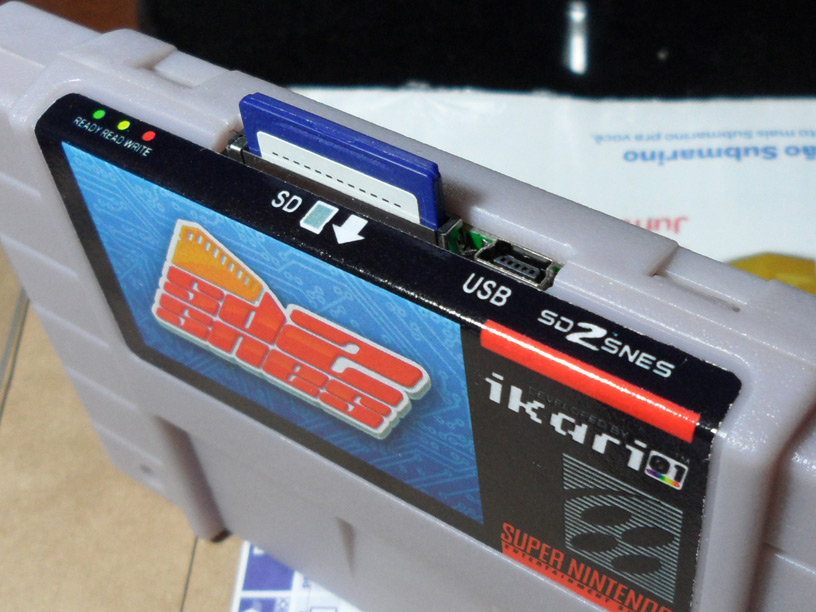
Now, with the PowerPak out and all I'm not sure anybody cares, but there has been some progress. A nice little PCB came out, and then one more with some fixes. And the third revision is on the way.

There are some pics
here.
Currently there's only Map 0x20, 0x21, and 0x25 support with near-time SRAM save.
I think the next step will be DSP-1 emulation.
There's a 200kgate Spartan 3 on the board which can be replaced by its pin compatible 400kgate variant, which should definitely be sufficient for chip emulation in case the former is not enough.
Quote:
There's a 200kgate Spartan 3 on the board which can be replaced by its pin compatible 400kgate variant, which should be sufficient for chip emulation.
Quote:
DSP-1 emulation.
nice. Bonus points for the SD card interface. How long does it take games to load? Say, what is the figure on a 32mbit ROM?
Looks to be a very capable cart, I'm wondering how much that SRAM is costing though =(
The fat FPGA is a huge plus, I'm guessing that's your main draw. Playing starfox on the real deal with a flash cart would be wicked.
smkd wrote:
nice. Bonus points for the SD card interface. How long does it take games to load? Say, what is the figure on a 32mbit ROM?
It's a good deal slower than the Powerpak, due to the AVR accessing the SD card in SPI mode.
A 32Mbit ROM takes about half a minute to load.
It should be possible to offload the bulk transfers to the FPGA which should result in at least a 100% speed increase. ATM the AVR uses its SPI to load a block from the card, then uses the same SPI to push it to SRAM via the FPGA. With the data flowing directly to the FPGA I have direct SRAM access (no shared SPI) and could achieve higher SPI clocks (currently 6.144MHz).
EDIT: to clarify, this is possible with a software update as the FPGA is already connected to the SPI bus.
Quote:
Looks to be a very capable cart, I'm wondering how much that SRAM is costing though =(
Quite a lot. :/Quote:
The fat FPGA is a huge plus, I'm guessing that's your main draw. Playing starfox on the real deal with a flash cart would be wicked.
True, that would be awesome. Still a long way to go though.
Just because the SNES PowerPAK came out doesn't mean there is no interest in other projects anymore. If anything it should encourage other projects to think about how to be different than it. I'm sure if GSU (SuperFX) support existed in a similar type of device they would find lots of interest and buyers.

Those SRAM prices are outrageous! FWIW, I'm excited about this cart.
SRAM makes the designing of any product easier but more expensive. With DRAM and SDRAM you must have a refresh cycle in your design. I think that PSRAM is supposed to do this for you so you don't have to worry about it yourself and it acts like SRAM.
If your memory is twice as fast as the CPU, I don't see how hard it would be to work DRAM into your design. The Apple II multiplexed CPU, video, and refresh with just discrete logic. On the Super NES, memory would need to be capable of 7.2 MHz operation for this to work in fast ROM mode.
FWIW I'm also interested in this cart. It will support add on chips. That's really cool.
I don't really know how hard it is. It's obviously not impossible since tons of SNES Copiers were made using DRAM. And as I heard the PowerPAK uses SDRAM. But by using some sort of memory that doesn't require you to refresh it like SRAM or PSRAM all you have to worry about then is a BIOS, Source for loading data and Memory Mapping functions for your device. So atleast you'd have one less thing to worry about.
I wouldn't mind waiting 15 seconds to load a 32mbit ROM if that means anything. Atleast when I play Mario Kart or some hack of it, it would only be a couple seconds waiting with no need for donor DSP-1 chip. I still have to import a NTSC deck though..
SRAM cost is clearly going to be killer (hope you got a decent quantity discount) but surely it would make stuff like SFX/SA-1 high speed ROM / RAM access easier to implement. I think I read in the docs that SA-1 runs at 10mhz when it has ROM or RAM to itself.
smkd wrote:
I wouldn't mind waiting 15 seconds to load a 32mbit ROM if that means anything. Atleast when I play Mario Kart or some hack of it, it would only be a couple seconds waiting with no need for donor DSP-1 chip. I still have to import a NTSC deck though..
SRAM cost is clearly going to be killer (hope you got a decent quantity discount) but surely it would make stuff like SFX/SA-1 high speed ROM / RAM access easier to implement. I think I read in the docs that SA-1 runs at 10mhz when it has ROM or RAM to itself.
Frankly I did not pay too much attention to cost. I don't have the guts nor time for commercial distribution anyway; being in Germany only makes it harder, with a f*ckton of regulations to meet. I do intend to release the source and gerber files at some point. (GNU GPL or similar)
Actually I need more than 7.2MHz of random access throughput. SuperFX and SA1 (among others) have separate buses for ROM and RAM which can be accessed simultaneously. e.g. while the SuperFX has the RAM for itself, the SNES can still access the ROM freely.
My board has only one memory bus so I need at least three time slices per "master clock" (roughly: AVR, SNES, GSU). With the FPGA maxed out at ~100MHz and an estimated 11 clocks per SDRAM access using autorefresh and autoprecharge, it would be a bit of a stretch. EDIT: This may be inaccurate, I haven't looked into the various SDRAM datasheets for quite some time now.
How many clock cycles does the SA-1 need for memory access? "The Documentation" does give some numbers for the SuperFX but not for the SA-1...
However, I'm considering it maybe for next year.

I like the idea as SDRAM is dirt cheap and having a single 64M or 128M chip instead of four 16M chips would save a lot of space. I'm kind of an FPGA noob so I need some time to make myself comfortable.
EDIT: I was a bit off, loading a 32Mbit ROM currently takes about 21 seconds.
The SuperFX is actually the simpler chip. It has a switch to toggle access between the S-CPU and GSU accessing ROM or RAM. The SuperFX2 side can access the ROM/RAM at 5 clocks per fetch, or 21.47MB/s / 5. But it also caches instruction reads in a 256-byte window, and can fetch from it at the full 21.47MB/s. If you aren't concerned with high accuracy, games should still work okay if you omit the instruction cache, they'll just run a little slow and music will end too quickly in some games.
The SA-1 is the real bastard. It can access ROM, I-RAM and the I/O registers at the full 10.74MB/s. It can access BW-RAM at 5.37MB/s. But both the S-CPU and SA-1 share the memory at the same time. There is a bus contention chip inside the SA-1 that detects this, and it will stall out the SA-1 until the S-CPU is done accessing it, as it obviously can't delay the S-CPU's request.
It's not the two chips accessing the same address at the same time that is a problem, but both accessing the same chip at the same time that will make SA-1 reads take longer.
So to get both of these right with only one SRAM chip, you'll need some crazy fast SRAM and some logic to determine which emulated memory chip each device is accessing at which time.
Thank you for the details, byuu.
So let me think.. my FPGA logic is currently running @86.02MHz, using 6 clocks for one SRAM access cycle, resulting in roughly 70ns per cycle or 14.336 Mwords/s. (Data width is 16bit on the SRAM side, which might be beneficial.) My SRAM is 55ns so there should be some headroom.
With FastROM, cycle length appears to be ~280ns, meaning I can do four 16-bit transfers "at 14.336MHz" each, with the first one being the S-CPU access to meet the required 120ns with some margin.
The documentation states that with the SA-1, the S-CPU must run at 2.68MHz, so I have ~372 ns between two S-CPU accesses which is enough to serve the S-CPU and run four more SA-1 cycles at full speed. Pausing the "virtual" SA-1 when a new S-CPU cycle is detected should not be too hard.
Having only one bus, I would also have to stall the SA-1 when they are not trying to access the same regions, where the original SA-1 would allow true parallel access (e.g. S-CPU -> BWRAM, SA-1 -> ROM). Resulting in only 7.16MB/s in this case. Damn! Does this happen a lot?
I-RAM (2kBytes iirc?) and registers (and the SFX's cache) will be implemented inside the FPGA as block RAM or maybe even distributed RAM.
But first things first, which will be an emulated DSP-1 in some sort of soft core.

Yay, I managed to offload the SD bulk transfers from AVR to the FPGA.
SPI clock is now 21.5MHz (as opposed to 6.144MHz) and Tales of Phantasia loads in 5 seconds. That's nice!
Quote:
Frankly I did not pay too much attention to cost. I don't have the guts nor time for commercial distribution anyway; being in Germany only makes it harder, with a f*ckton of regulations to meet. I do intend to release the source and gerber files at some point. (GNU GPL or similar)
that's a shame, I'd definitely be one of the guys willing to fork out for something as cool as this. I say that as a gamer/homebrewer though.
You said you want to release the source files at some point, and though I had to google what a gerber file is, it looks like I'd be able to produce a cart for my own use with these files. I wouldn't mind having one or two of these for personal use, what type of money would I be looking to spend to make it actually happen if you have any ideas? Where would I have to order from and what potential difficulties would I run into? Just curious, it'd be great to have something like this for myself even if you won't be handling the production yourself.
My first message here..
I did build a flash cartridge in 2004 (flash, SRAM and an ispGAL) based on Chnowack work. It is like the tototek board, programmed with a parallel port board.
I'am looking on the internet for documentation in order to build my own "yet another SD card cartridge". Ir differs from your board, I will use flash memory again because it is not expensive and I do not need to reload a game at each boot. I plan to use a cpld because his program is static. And like you an atmega to read the sd card (but i will try to use the SD parallel interface wile wiring the port with SPI in case of a problem).
The concept would be: the snes cpu reads NOPS, MOV, and JUMPS instructions coming from the cpld thus loading a "boot" program in SRAM. Once the program is in SRAM, the snes cpu jumps to the boot program and the cpld becomes configured in HiRom address space, giving only a tiny interface to acces the atmega in order to read the SD card.
The snes checks for an input, if say R buton is pressed it starts the FAT16/Menu/programming routines, else it looks for a lorom header in the flash memory and configures the cpld for lorom/hirom and removes the SD interface. Then the snes cpus clears his sram memory and jumps to the start of the ROM.
I do not know if the snes can execute program from his own sram? Anyone?
Thus no super FX on this, no nothing except maybe a fun DSP-1 simulation. Guess how.
I have indeed questions concerning your design. The fpga needs a "long" time at start to load his configuration. How do you manage the snes cpu read operations during this time? I assmume that the microcontroler controls the level shifter buffers between your board and the console?
Or maybe the micro controller holds reset signal enabled?
Why do you need to access your rom memory between 2 read operations of the snes cpu?
Why did you transfer the data from the avr to the fpga using SPI? You could have used a 8bit port, rd/wr signals and an interrupt pin from the atmega. It could have been faster.
If I understand, the super FX has on one side the snes bus and on the other side the ROM "bus" and therefore can cut the access to the snes?
Thus if this is correct your fpga cuts also the bus and you could send NOPS and JUMPS on the snes bus while loading the SRAM on the ROM side.
However I begin to understand and I find it simpler to load the "ROM" using the snes cpu throug a temporary custom atmega buffered interface at say $30 | $3000. Maybe it is slow?
How do you load your boot program?
Now with the built in SPI interface, do you need the avr?
How much time did you spend on this project? Because It took me a year and half to complete my flash cartridge. And the biggest problem with electronic is when you are stuck with an unexpected problem for month.
In my case it was parallel port glitches and time outs, the other problem is to get 1mm thick boards instead of the standart 1,6mm.
Nice project (but really big because of the SA, fx chip and co).
PS: design fever today....

smkd wrote:
what type of money would I be looking to spend to make it actually happen if you have any ideas? Where would I have to order from and what potential difficulties would I run into? Just curious, it'd be great to have something like this for myself even if you won't be handling the production yourself.
I can only tell you what I paid in Euros, you might get things cheaper in the US. (If you are in the US
)
The most expensive part is the PCB when you order just one or two of them. I paid around €120 for my latest prototype PCB (sans parts). Had I ordered 4 it would only have cost me €20 more. Maybe you can organize your own omnibus order (is that the correct term?) when it's ready.
I ordered the PCBs at pcbcart.com.
Parts amounted to about €95 (SRAM €60, FPGA €15, AVR €5, SD card slot €4, level shifters €3, voltage regulators €3, plus small change).
I ordered the parts at reichelt.de and rsonline.de, but they are German distributors. digikey.com might be a good choice.
Patrick FR wrote:
I'am looking on the internet for documentation in order to build my own "yet another SD card cartridge".
They spring like mushrooms these days.

Quote:
I do not know if the snes can execute program from his own sram? Anyone?
It's DRAM but yes it can.
Quote:
Thus no super FX on this, no nothing except maybe a fun DSP-1 simulation. Guess how.
Software emulation using the AVR, triggered by IRQ?
I structured your questions to make reading the reply easier without using tons of quote boxes:
Quote:
- The fpga needs a "long" time at start to load his configuration. How do you manage the snes cpu read operations during this time?
- I assmume that the microcontroler controls the level shifter buffers between your board and the console?
- Why do you need to access your rom memory between 2 read operations of the snes cpu?
- Why did you transfer the data from the avr to the fpga using SPI?
- If I understand, the super FX has on one side the snes bus and on the other side the ROM "bus" and therefore can cut the access to the snes?
Thus if this is correct your fpga cuts also the bus and you could send NOPS and JUMPS on the snes bus while loading the SRAM on the ROM side. - How do you load your boot program?
- Now with the built in SPI interface, do you need the avr?
- How much time did you spend on this project?
- Indeed, by holding the /RESET line on the cartridge slot.
- partly. It can control the direction of the block containing the SNES /RESET pin. Thus, it can reset the console and it can also detect when the user presses the Reset button on the console. SNES Databus /OE and direction, and SNES /IRQ direction are handled by the FPGA.
- To access the SaveRAM area which resides in one of the SRAM chips. I do it to monitor the SaveRAM contents and save to SD card when a change is detected. I need to time multiplex it because I only have one memory bus.
- Because I ran out of I/Os on the FPGA and was too lazy to switch to a larger package. Also, it makes for a flexible configuration/command interface.
- Not exactly. The SNES CPU has to cut access to the ROM itself (by granting the SuperFX access to it).
- I load it like a normal ROM during the initial reset phase.
- I keep it for flexibility. It configures the FPGA in serial slave mode, loading the bitfile from SD card. It will be preprogrammed with a bootloader so it can flash upgrade itself. So it's really easy to deploy upgrades. It gives me a nice debug console via UART. And there already exist great SD card access code written by the author of sd2iec, and FAT access libraries.
- I started in April 2009. I do it besides my normal job so real productivity mostly occurs when I'm on a leave.
Quote:
Software emulation using the AVR, triggered by IRQ? Smile
Right, and the avr being slower than the DSP1 in terms of clock cycles per multiply I am curious about the result. Some latches are needed in the cpld in order to handle the accesses. The PIC32MX could be better here: many times faster, multiply and divide and a slave parallel port of 4 addressable bytes. But this may be a shameful overkill (72Mhz Mips).
Quote:
Indeed, by holding the /RESET line on the cartridge slot.
Simple and efficient, I feared to use this before checking that it has a pull resistor up but indeed.

Quote:
To access the SaveRAM area which resides in one of the SRAM chips. I do it to monitor the SaveRAM contents and save to SD card when a change is detected. I need to time multiplex it because I only have one memory bus.
Tremendous, by the way the SD card would not tolerate million writes. Do you use a brown out detector to trigger the write to the SD? A timer?
Quote:
I keep it for flexibility. It configures the FPGA in serial slave mode, loading the bitfile from SD card.
I did not know that it was possible with a xilinx to lad the configuraiton trough SPI. Loading from the SD is a very good idea because it simplifies development, allows updates, and avoids the cost of an SPI memory.
Thank you for all these explanations. Your design is what would be the ultimate snes cartridge because of the fpga.
When thinking the design I feared to use an fpga because of this load step and configuration memory size. You solved the problem in an elegant way.
But yes it is a lot of work, I do not know if I will develop my SD cartridge yet because of the work required but it is interesting because it allows to learn things fast.
PS: Chnowak multi console copier that I used to start (it simplified a lot my work):
http://chn.bplaced.net/index.php?doc=mcc/mcc.html
Quote:
Patrick FR: However I begin to understand and I find it simpler to load the "ROM" using the snes cpu throug a temporary custom atmega buffered interface at say $30 | $3000. Maybe it is slow?
I was wrong then, I thought of a complex system loading the ROM in parallel of the snes execution.
With the cpld I will be obliged to use a trick at boot time with the snes cpu to load the boot code because the cpld has not enough pins to address the Rom and Sram. And maybe not enough complexity even if it had enough pins.
Maybe it wont fit at all, I must begin with the cpld.
Quote:
Quote:
I do not know if the snes can execute program from his own sram? Anyone?
It's DRAM but yes it can.
Very useful then.
Today I read from
http://sneshack.blogspot.com/ that it would be nice to pause the snes using only jumps to a specified addresse and indeed NOPs are not usefull.
By the way, many people are "working" on the nearly same thing.
Yes, SaveRAM access is not directly passed through to the SD card.
The AVR permanently generates a checksum of the memory area. When a change is detected, the SaveRAM will not be saved to SD card until it has remained unchanged again for about 1 second.
Of course there are some games which use the cartridge RAM as work memory, i.e. update it constantly. In this case there's a fallback that will save every ~30 seconds even when contents keep changing.
And there's a manually triggered save when resetting to the menu by pressing Reset on the SNES for more than 1 second.
koitsu wrote:
Sorry, kinda zonked out when I got home.
kyuusaku is correct, re: Fast/SlowROM times. "Normal speed" (e.g. "SlowROM") has to be 200ns or faster. "High speed" (e.g. "FastROM") has to be 120ns or faster.
This is defined in the manual, section "Super NES Software Submission Requirements", chapter 1. Revision C, dated 1992/11/02.
I'm a bit confused. Why is it requiring speeds at that rate?? Master clock /6 = 280ns per memory cycle and /8 is 372ns per memory cycle. Why would you need anything faster than that? All the SFX docs I've read stated VDMA doesn't move data from the bus any faster than master clock/8 per byte, so that can't be it. Unless this speed rating is for one of the addon processors or DSPs...
As I understand it, you need the ROM to respond within about half a memory cycle. /OE goes low on a read, and the data lines need to stabilize before it goes back high.
tepples wrote:
As I understand it, you need the ROM to respond within about half a memory cycle. /OE goes low on a read, and the data lines need to stabilize before it goes back high.
The SNES needs a rom to respond the rom to respond and have the data on the bus at
half a memory cycle!? Why? That doesn't make any sense. I don't know of any other 65x related processor setup that requires that. It also defeats the whole purpose of a slower clock speed (slower memory speed means slower roms, means cheaper roms). I've always used roms slightly faster than the memory bus speed (for 65x), but never twice as fast. The state from off to enabled for /OE is tiny in comparison to the rated chip speed for roms. The propagation delay is really small. There's something that's missing here.
This was made a while ago for a different purpose, but anyway:

/OE ("/SNES_RD") stays high on hw register access (where /PARD should go low).
The large pause is the refresh cycle that occurs in the middle of each raster line.
To the right we see a single SlowROM cycle. (probably WRAM access)
/OE appears to be derived from the "CPU clock". It is low for about t_cycle-140ns. So in FastROM operation, it is low for ~140ns, in SlowROM operation it is low for ~230ns.
About 20-30ns after it goes high, the new address is put on address bus A (haven't looked at the B bus so far). Nothing else seems to happen on the memory bus during that period. There seems to be no bus sharing within the same cycle.
EDIT. This should clear things up. In the original 65C816 design, there are only 16 address lines - BA0-BA7 (A16-A23) are multiplexed on the D0-D7 lines.
see
http://www.westerndesigncenter.com/wdc/documentation/w65c816s.pdf p. 13 and p.26.
Oh thanks for the capture pic. I see, it's because they multiplexed the upper address lines on the data bus lines. That makes perfect sense. I totally forgot the original '816 was supposed to be pin compatible with the 65x. That's the only way to extend the address lines while still maintaining the original pin count. Although, that's really stupid on Nintendo's part. If anything, that explains why the CPU speed is so slow. Because of requiring double the speed memory. Man, Nintendo really screwed up on that one :/ They definitely should have went with a custom core processor like Hudson did. And I can't believe WDC still uses mechanism. Just another crippling mechanism added to the mistakes of the '816 IMO.
Small(?) update:
I am going to switch to PSRAM after all
A 128Mbit chip is only 1/5 the cost of my current 64Mbits of SRAM and we managed to get the small BGA package soldered with an, uhm, super special custom reflow pizza oven!
There will also be a second bus with 4Mbits of SRAM to facilitate parallel access for custom chips without getting into timing trouble.
The uC will be upgraded from AVR to an ARM based architecture, which gives much more bang for the buck and should further improve loading speed and provides a hardware USB interface, too.
I am also looking into adding an audio DAC to the board, maybe to provide compatibility for byuu's 21fx spec, or just to be able to emulate other sound chips, who knows
I hope to connect all PA lines, but I still need to recalculate the available I/Os on the new FPGA (will have to upgrade to a 208-pin package anyway for the 2nd memory bus).
Soldering SMDs actually work using toaster ovens? Can you please describe how you did it (I have seen it discussed on forums before but never explained).
Well, I usually hand-solder SMDs where the pins stick out. But with BGAs that was not an option
It is possible but you need to closely observe the temperature in the oven. Chip manufacturers usually recommend a temperature profile that looks a little bit like a backward ADSR envelope. e.g.:
http://www.actel.com/documents/Solder_Reflow_LeadFree.pdf
Basically there's a preheating phase to preheat the components and activate the flux, a solder phase where the temperature stays above the melting point of the solder used (but below the allowed peak temperature), and a cooldown phase. For leadfree solder balls used in RoHS parts, the melting point is usually 217°C.
I simply used the thermometer function of my multimeter and put the sensor in the oven along with an empty board. On the board I placed a small amount of leaded solder (melting point=183°C) and a small amount of leadfree solder (melting point=227°C). Yes, this is a different melting point from the number I gave above because I saved a few Euros and purchased silver free solder which has a 10°C higher melting point.
I then used Manual PWM™ to slowly ramp up the temperature in the oven and noted down the multimeter readouts where the leaded and lead free solder melted, respectively. The MM actually read some degrees less than what the actual temperatures should have been according to the given solder specs.
Using this I was able to extrapolate the "MM temperature" that I needed to reach. My goal was to stay between 230° and 240° for at least one minute, so that was about 224°-234° on the MM.
I then put the board with flux and
the BGA chip on it (align carefully!) into the oven. Heated it slowly, stayed below ~180° for 2-3 minutes, then ramped up to 230° and tried to stay there for a minute. Afterwards I switched the oven off and let it cool with the oven door shut. Et Voila!
And it even worked. Here's a
pic of the test board wired to an existing sd2snes prototype. The four fat SRAMs that still reside on the board are disabled and now obsolete. Note the difference in space requirement, i found it pretty cool.
Note that this is quite a taxing task, because having to turn the oven switch while observing the MM readout and trying not to move the (light, cheap) oven too much is not so easy and definitely not recommended for more than experimenting
I'm going to build an automatic temperature control according to
http://thomaspfeifer.net/backofen_smd_reflow.htm (sorry, it's in German) to have an uC do this hopefully much more accurately.
Small update for the record.
BGA reflow soldering proved feasible. So there will be 128Mbits of 16-bit PSRAM + 4Mbits of 8-bit SRAM on the secondary bus.
A DAC for the SNES's analog line in will be included. (Testing the DAC is the last todo before a prototype PCB is ordered)
The B address bus is fully connected, who knows what it may be good for.
There's a replaceable backup battery for RTC support and SRAM data retention (I'm sure there is some good use for that)
And of course, a SuperCIC key
enabling operation on any unmodded SNES/SFC, but also adding the option to switch 50/60Hz via software on SuperCIC modded consoles.
MSU-1 support may or may not be possible depending on the data rate I can get from the SD Card.
Two of the LDOs have been replaced by a dual switching regulator, slightly improving power consumption. This will be more important once the FPGA core becomes more active due to custom chip emulation.
Quote:
MSU-1 support may or may not be possible depending on the data rate I can get from the SD Card.
:(
In that case, would it be possible to support the MSU1 audio interface only? Just leave the data busy bit as always set.
I imagine a lot of uses would be for audio-enhancement only, including my Der Langrisser CD-audio patch.
Quote:
And of course, a SuperCIC key
Soooo need a SuperCIC cartridge dumper about now for those pesky SA-1 titles :D
byuu wrote:
Don't

yet, there is still hope!
Quote:
In that case, would it be possible to support the MSU1 audio interface only? Just leave the data busy bit as always set.
Sure thing. Even compressed audio should be possible.
I had no idea MSU-1 support was planned for this. would love to see that stuff running on a real system. Even if it was just audio.
Here's a video demonstration of the cartridge sd2snes with the support MSU1
720p available
http://www.youtube.com/watch?v=EqXYPvhHMCo
kogami wrote:
Here's a video demonstration of the cartridge sd2snes with the support MSU1
720p available
http://www.youtube.com/watch?v=EqXYPvhHMCoWooow!
This looks (and sounds) incredibly awesome! Where's the order button?
Who made this music, BTW?
Can't wait to see this finished and released!
So your flash cart supports Byuu's mass storage idea which has a Der Langrisser patch for? If that's so that's awesome. Also you mentioned custom chip emulation which sounds awesome.
A very cool video for animated sequence MSU1
http://www.youtube.com/watch?v=yULkopwR8oA
Very nice! I want one.
Is the MSU1 only good for streaming FMV and audio or can it enhance in game graphics as well?
It is basically a 4GB data stream that can allow DMA directly into video RAM.
This can speed up processing: no need to waste CPU cycles decompressing graphics to fit into tiny ROMs. It can also enhance visuals: upload a new sprite animation every single Vblank. Games can store almost unlimited levels, so long as they upload levels to RAM first.
Maybe this thread should be split ("What is the largest sane SNES ROM size?" vs general sd2snes discussion) or subject changed to "sd2snes" or something.
PM me the URL of the split point (right-click the little page next to the post date), and I'll split it for you.
This projects sounds really impressive, if indeed he can get those chips to run! Hope he or someone decides to produce them for sale though. Other wise, not so interesting.
Wow this looks like it will be so cool. Ultimate snes card if it supports all enhancement chips like superfx, dsp1, Cx4, etc. Also Not sure what all would be involved but satellaview support would be sweet. I'm sure that would probably be a whole new level of complexity and is probably more of a snes mod (like Ultra16). What ever the case keep up the good work would love to see another genius ikari project from ikari.
Satellaview support is already implemented
However some games, most notably the Zelda Inishie no Sekiban series, cannot be played (without patching) because they rely on data that was downloaded from Satellite to RAM during the actual broadcasts.
Oh, and S-RTC support is in. Time is supplied by the RTC integrated in the µC.
..pr0n!
I have some questions if you don't mind answering them
1. Will you mass produce and sell them? If yes; when?

2. Does it support all special chips?
3. How far in the development process are you?
Got myself a snes powerpak, but still...I'm interested to know if you will produce sd2snes units
Finished the uPD77C25 core. DSP1-4 work fine.
(DSPx roms required.)
There will probably be a first batch of 100 sd2sneses this year, maybe another 100 next year. Not so sure yet.
> Finished the uPD77C25 core. DSP1-4 work fine. Smile (DSPx roms required.)
Neat :D
Is there enough memory to support the ST-0010 and ST-0011? It needs 52KB instead of 8KB per game, but the instruction set is the same, just with a new jump mechanism.
If not, I believe we can get ST-0010 support in there by intentionally trimming the ROM (it's 90% padding) and treating it like a 7725 instead of a 96050. That game barely uses the chip at all.
Also, if you haven't stopped by my forum recently, we were able to RE the Hitachi HG51B169 (Cx4) for MMX2/MMX3. The program ROM is stored on the mask ROM, and you only need 0x1800 bytes for data RAM+data ROM. It does have a high clock rate though, 20MHz. May not be worth the work/FPGA space for only two games.
> There will probably be a first batch of 100 sd2sneses this year, maybe another 100 next year. Not so sure yet.
Awesome! Please save one for me to buy :D
Quote:
Awesome! Please save one for me to buy
+1 on that.
Quote:
Is there enough memory to support the ST-0010 and ST-0011? It needs 52KB instead of 8KB per game, but the instruction set is the same, just with a new jump mechanism.
Sadly no, the FPGA has roughly 36kB of block RAM. 17kB of those are always dedicated to MSU1 for data+sound buffers (MSU1 should be supported alongside any custom chips).
Now I could theoretically use both my external memory chips combined to fetch a 24bit instruction in a single cycle but I doubt I can get to 8MHz core clock with that (the SNES must access both buses quasi-simultaneously and one of the memory chips is only 70ns).
About the CX4 (AWESOME feat, read a lot about it!) - Doesn't it also have an internal program RAM where it copies one 512b "page" from the mask ROM prior to execution? Or does it fetch directly from mask ROM? How is SNES ROM access handled then? Or does it have a switch like the SuperFX?
I think I should read the source already...
Quote:
Sadly no, the FPGA has roughly 36kB of block RAM.
Drat. Okay, if you want to try and get F1 ROC II running anyway ... try this.
Cut the first 6KB of the ST-0010 ROM to a new file, this will be the program ROM. Now go 48KB into the file, and copy the next 4KB into our new file. This will give you a 10KB file similar to the other dspN.bin files, only it'll use an extra 2KB of data ROM. See if F1 ROC II will run using your 7725 core @ 8MHz, I believe it will. It does not use any new opcodes, the only obvious thing is that it needs one extra bit on the data ROM pointer address.
st0010.bin only has 0x640 bytes of PROM, and 0xbe0 bytes of DROM.
Quote:
Doesn't it also have an internal program RAM where it copies one 512b "page" from the mask ROM prior to execution? Or does it fetch directly from mask ROM? How is SNES ROM access handled then? Or does it have a switch like the SuperFX?
Yes. It has to buffer in the first page as well. You can load in pages from the SNES or Cx4 side. I don't know yet if the SNES side can load in both pages or just the primary/active one. I also don't know how the buffering works from the Cx4 side. My guess is the chip freezes until the buffering is finished.
The mask ROM is completely inaccessible to the SNES while buffering is under way. The Cx4 takes over the ROM chip to do its own buffering as needed. It doesn't appear that access is restored until the Cx4 hits a halt opcode. So you're pretty much fucked if it gets stuck in a loop I guess.
The Cx4 also has a simple DMA that can move mask ROM into Cx4 RAM. This also locks out the SNES CPU from accessing the ROM (and presumably the Cx4 RAM) while it is active.
And lastly, it allows vector override. Write new vectors into $7f60-7f, and when the Cx4 is active, it will give those values for $ffe0-ffff for NMI/IRQ support. MMX2/3 don't seem to use this feature, though. It just turns off all interrupts prior to executing a function.
-----
I do love the clock speed, the instruction set, and number of registers. But this chip honestly sucks compared to the uPD and SA-1 in terms of power. Having to multi-task out of work RAM is really shitty, and 256-instruction pages are much too small.
Trying it out now.
Do I also need to map the data RAM?
For the chip to function, no. It only communicates with the SNES via DR/SR, just like the DSP-n chips.
However, it does use the mapped data RAM area as non-volatile save RAM. Basically just map that in like regular cartridge SRAM and it should be fine.
Hm, looks like it communicates exclusively via DP. I logged all dsp accesses in bsnes and DR/SR are not touched even once by F1 ROC II. However once the race starts, there's a firework on DP.
I guess I'll have to implement it then
ST0010 now works.
Had to up the DataRAM size from 256 to 1024 words and make it shared between the uPD and SNES.
Ah, guess I was wrong after all. Sorry about that :(
Glad to hear that it works though, great job! I was hopeful you could get it to work, given how small the program ROM turned out to be.
We'll have to leave the ST-0011 to the emulators for now. That thing is a real beast, and you really need all 15MHz since it's a Chess AI.
Evil idea:
The ST0011 program ROM uses only 410 different instruction words... so I could reduce the instruction size to 9 bits and use a LUT. Of course that's far from a universal approach.
It would still require cutting MSU1 support for ST0011 but it might be better than nothing (except, well, it's just some Shogi game

)
EDIT: ugh, disregard that... I counted only among the first 2048 instruction words.
Now there are 2139 different instructions.
More info on Cx4:
Cleaned source code @ snes/chip/hitachidsp in:
http://bsnes.googlecode.com/files/bsnes_v079r04.tar.bz2
(vector override portion is not used by MMX2/MMX3)
Hardware requirements:
0xc00 bytes data RAM aka IRAM
0xc00 bytes data ROM
~0x200 bytes registers and MMIO stuff
Technical requirements:
24-bit registers with 24-bit signed multiplication to 48-bit result
Roughly 32 or so unique opcodes, all very simplistic
Has a DMA mode that transfers from ROM to IRAM
Either the SNES or the Cx4 has control of the ROM/IRAM, never both
It's safe to always allow SNES ROM/IRAM access, so long as it won't stall out the Cx4
Program ROM is inside the game itself. You can either buffer in 2x512-byte pages, or fetch on demand. The former is more correct, but the latter works fine as well.
Wants to run @ 20MHz, but it can be safely under-clocked a good bit, from what I hear.
Anyway, it seems like you are well on your way here to an official release. I'm not suggesting you expend effort on Cx4 support or anything, unless you really want to.
But if you do want the chip support, let me know if I can be of any assistance :D
ikari_01 wrote:
It would still require cutting MSU1 support for ST0011 but it might be better than nothing
Do you mean only that one game could not use ST0011+MSU1 at the same time? Or that you'd have to remove it entirely to support it? If the former, not a big deal. If the latter, ;_;
The first one's easy to get anyway if people really want to play it. But I mean there's probably two people in the world interested in playing it anyway. F1 ROC II on the other hand seems pretty popular, Lord Nightmare is a big fan of it.
Quote:
EDIT: ugh, disregard that... I counted only among the first 2048 instruction words. :( Now there are 2139 different instructions.
ST-0011 is an absolute beast. The most powerful coprocessor (sans maybe the ST-0018), and utilized almost 100%. It also really wants to be run at 15MHz. You can probably get away with 8MHz, but AI moves would take twice as long. You'd have to hack the title screen to read "遅指し 二段 森田将棋" :P
Haha don't worry. I'd never ax MSU1 for one custom chip. If I had to decide I'd rather ditch ST0011 completely.
I meant disable MSU1 when ST0011 is used.
And of course I want to support Cx4. Mega Man X2/3 are essential IMO.
Even if I don't finish it now, sd2snes can flash itself from SD Card, so I'm expecting a variety of features to arrive after release anyway.
Anyway, thanks for all the details on the Cx4. It seems very nice to implement instruction architecture wise.
About the ST0011: I have the 7725 core running @13.71MHz (96/7) at the moment anyway, so 15MHz (would be 16MHz then) is probably not a far cry. However ST0011 doesn't have top priority now.
Also LOL @遅指し
Ah btw, how is the DataRAM split up with the ST0011? F1 ROC II seems to use the lower half of the ST0010's DataRAM for data exchange between the DSP and SNES, and the upper half for storing save data.
That's a good question. I'm afraid I haven't looked at Morita Shougi 1 any more than necessary to get it playable, heh. It's a very boring game.
The flashing thing sounds cool. Lots of potential there for Cx4, OBC1, S-DD1 (proper - for SFA2) and SPC7110; perhaps some entrepreneurs will take a stab at it for you, ala the Retrode's dumping adapters.
Got the 7725 core cranked up to 19.2MHz... now what to do with it ^^;
F1 ROC displays one line of garbage in the upper half of the screen now, everything else still works perfectly. There was no real point in doing it, though. But that will give me enough additional headroom for the opcode LUT handling in case I decide to implement ST0011...
What is it exactly that the OBC1 does, and for what purpose? From skipping through bsnes source it looked like it just shuffles some addresses around when cart RAM is accessed, based on register settings.
The OBC1 is just a glorified bit twiddler used for building OAM (sprite) tables. Each sprite has 34-bits of data, and the last two bits can be a pain to access for individual sprites, because they are all packed into a separate buffer.
It seems like an absolute waste of money, some better code optimizations would most certainly allow Metal Combat to work with only the base hardware.
ikari_01 wrote:
There will probably be a first batch of 100 sd2sneses this year, maybe another 100 next year. Not so sure yet.
Assuming the cost is under $500, sign me up for one. I am most interested in the DSP emulation. It is nice to see somebody finally creating a SNES flash cart that won't require destroying retro-gaming hardware.
Are you going to get a nice plastic shell designed and fabricated for sd2snes? If you are mainly interested in designing the perfect technology and don't want to be overly troubled with business stuff, consider teaming up with RetroZone. While they already sell the SNES PowerPak, they could sell a product based on your sd2snes as a higher-end alternative to the PowerPak.
To whom it may concern: I put up a little blog documenting the current status and progress
http://sd2snes.de/
You implemented CX4 core in your cart design? That's awesome! Wasn't expecting that kind of thing. As far as I know that's something no other commercial flash cart maker ever implemented. My god, last time I checked on this project long time ago I just thought it would end up just being a fun project for you duplicating the basic functionality of an everdrive or powerpak. I just say the list of core you implemented and the one planned. All I have to say is Wow. Keep going like that and I reckon you will be creating some serious buzz and interest among the retro gaming community. I wasn't excited about a SNES flash cart in a while but that seriously did the trick.
I'm running a batch of 100pcs in the course of 2012, starting end of March. The hardware is now declared final
Most units are already reserved but there's still a small quantity left. If you're interested drop me a private message here or via
http://sd2snes.de/blog/contact .
EUR 120 + shipping (depending on country of destination). It ships as an assembled PCB in an ESD bag, bubblewrapped, in a cardboard box.
Be prepared to wait though - I'll be making this batch by hand so I can only make ~3pcs per week
And that's it - all are gone.
Everybody who wrote me has made it on the list, even though I haven't replied to all messages yet. I hope to answer all messages within the next two days.
Looks like I missed out, Bummer.
Oh well. Stuck with BSNES for now.
ikari, was there any chance of you "licensing" the design for other larger operations to make?
Possibly there is. Stay tuned.
Looks like StoneAgeGamer is organizing a proper mass production, which is good because ikari's time is better spent improving the firmware:
http://www.facebook.com/StoneAgeGamer
Hopefully everybody plays fair and money from sales is fairly distributed.
It will be Krikzz, Mr. Everdrive, handling the production, he just posted that on his forum! Will be the "Ferrari" $$$ of SNES flash carts though.
When this us mass produced I will likely choose is over a powerpak. I love my nes powerpak but this is much more advanced than the snes version.
Super-Hampster wrote:
When this us mass produced I will likely choose is over a powerpak. I love my nes powerpak but this is much more advanced than the snes version.
Supposedly the price is going to be like $170 though. Honestly, that is just ridiculous.
3gengames wrote:
Super-Hampster wrote:
When this us mass produced I will likely choose is over a powerpak. I love my nes powerpak but this is much more advanced than the snes version.
Supposedly the price is going to be like $170 though. Honestly, that is just ridiculous.
Actually I think $170 is a good price. I was afraid with all its features and abilities that it would be more than that. The snes powerpak is $155, $140 at the moment on sale, and can't do all this one can. I'm pleased with $170 if that is the final price.
3gengames wrote:
Super-Hampster wrote:
When this us mass produced I will likely choose is over a powerpak. I love my nes powerpak but this is much more advanced than the snes version.
Supposedly the price is going to be like $170 though. Honestly, that is just ridiculous.
It's not really that insane, the electronics in it cost a bit more than those in the PowerPAK so naturally it will cost more.
I just received my SD2SNES today! I was surprised at how fast it was delivered, I'm used to waiting 2-3 months for things I order abroad, but this came in less than a month! And directly to my home too, which means no abusive taxes! Yey! It was the exact opposite with the PowerPak.
Anyway, I'll be playing with it later tonight, do you guys have any tips on how to deal with the thing? I haven't done anything yet, I didn't even download anything, so I figured I'd just ask if you guys have any advice on setting it up.
...No love for the SD2SNES then? Do you all have SNES PowerPaks?
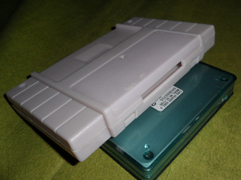
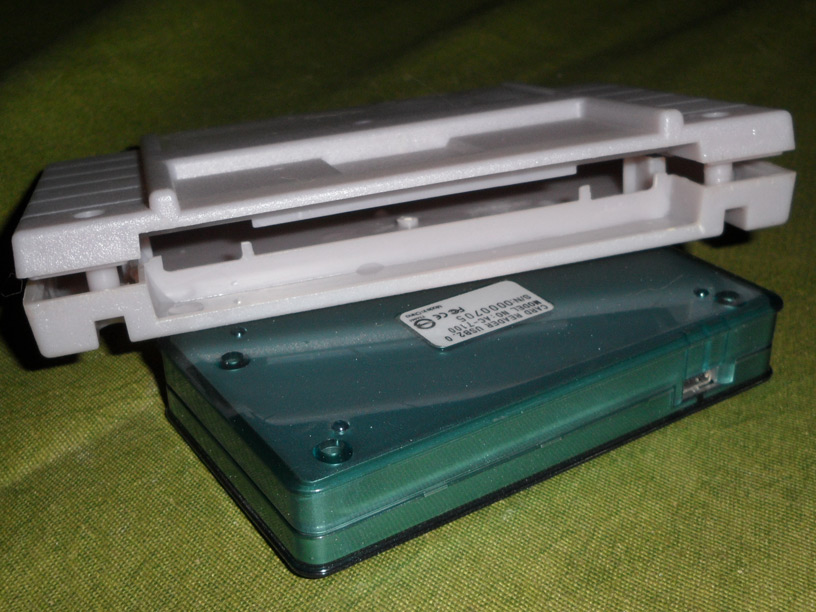
Well, I'm going to hack a cartridge case now, I think it's a bit risky to insert the bare PCB into the console, with the plastic flaps forcing against it and all. Afterwards I'll check the software side and finally test it.
tokumaru wrote:
...No love for the SD2SNES then? Do you all have SNES PowerPaks?
I guess a lot of us do, except for geezers like koitsu who still use floppy copiers. Some people buy the first solution that works for a particular purpose.
Quote:
Well, I'm going to hack a cartridge case now
I understand it's different in countries with prohibitive import duties, but that's why I bought the "deluxe" version of the (MD) EverDrive, because it comes in a known working case.
tepples wrote:
I understand it's different in countries with prohibitive import duties, but that's why I bought the "deluxe" version of the (MD) EverDrive, because it comes in a known working case.
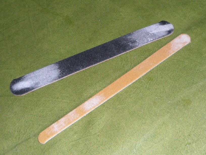
Yeah, since I was unsure whether this would be taxed or not, I decided to go as basic as possible. I've become pretty good at opening holes in cartridge cases, and all I use is nail files. Here's the result:
Attachment:
 sd2snes-case-1.jpg [ 130.62 KiB | Viewed 4954 times ]
Attachment:
 sd2snes-case-2.jpg [ 151.09 KiB | Viewed 4954 times ]
And here are the "tools":
Attachment:
 sd2snes-case-3.jpg [ 211.5 KiB | Viewed 4954 times ]
I'm not sure if I'll open holes for the LEDs, since that would mess with the label.
when I made my shell I also relocated the leds:

The position of the LEDs is indeed don't play well with the US cases. For now I'll just keep them hidden. Yours looks great!
My label-making skills aren't that great either... I couldn't find a place that would print on glossy sticker paper, so I went with the non-glossy one and used paper varnish to make it glossy, but it made the brighter parts of my Everdrive label a bit transparent, and since the Genesis cartridge case is black it ended up darkening certain spots on the label.
I printed 3 copies of each label though (Mega Everdrive and SD2SNES), so now I'm trying a different kind of varnish... The one I used previously is a liquid you apply with a brush, and this one comes in a spray can. From my tests it doesn't look as glossy, but if it protects the label without making it transparent I guess it's OK.
I never got a SD2SNES because the only significant bonus would be the MSU-1 support. I already own the special chip games that it supports like Mega Man X2 & X3.
I guess that the advantage of the SD2SNES is that it has the potential to support all the expansion chips, even though it doesn't currently.
While that's true, over 90% of SNES games use no special hardware. Only a small minority does. The only truly unaccessible game that could be supported is Star Fox 2 which was never released. But it's not that hard to make a hacked cart with it. Also technically one of the ST chips I think ikari said wouldn't be doable, something about hardware limitations. I think what most people want to see is Super FX and SA-1 supported. Those were the most prevalent chips after DSP1 I believe. I'm sure SDD-1 should come along eventually. But we're still talking about only a handful of games. Obviously notable ones like Kirby's Dreamland 3, Kirby Super Star, Mega Man X2/X3, Super Mario RPG. Though I do understand that people from certain parts of the world have alot harder time getting access to those games so support in the cartridge would be a big deal.
MottZilla wrote:
Obviously notable ones like Kirby's Dreamland 3, Kirby Super Star, Mega Man X2/X3, Super Mario RPG. Though I do understand that people from certain parts of the world have alot harder time getting access to those games so support in the cartridge would be a big deal.
Yeah, to me that makes a difference. I really like the Kirby games (and the Mega Man games too, but not as much
), but whenever I find one of them for sale they cost US$40 or even more. Sometimes there'll be a beaten up cart with a nasty label that costs less, but there's no fun in collect that. I don't know why, but SNES carts are ridiculously pricey around here, much more than Genesis/MD ones, so it makes sense to buy an SD2SNES instead of 4 or 5 of these expensive games.
tokumaru wrote:
I just received my SD2SNES today!
Congratulations, and welcome to the club!
Without question, the sd2snes is the unrivalled, top of the line SNES flashcart currently available. ROM loading is lightning-fast, even 32 Mbit games start almost instantly. There's a real time clock built in, which (apart from adding support for more games) makes it easier to synchronize SRM files. BTW, the hardware looks more "real" and professional than any other unofficial/third-party SNES accessory I'm aware of, right down to the exact shape and color of the PCB and edge connector.

Plus, the original creator is still actively developing the firmware, which I guess is worth noting.
tokumaru wrote:
Anyway, I'll be playing with it later tonight, do you guys have any tips on how to deal with the thing? I haven't done anything yet, I didn't even download anything, so I figured I'd just ask if you guys have any advice on setting it up.
Setting it up is easy, just
download the latest firmware and follow the instructions on the same page. Also, have a look at the
card list to see what type and brand of SD card to go for if you require stable MSU1 support.
Have fun!
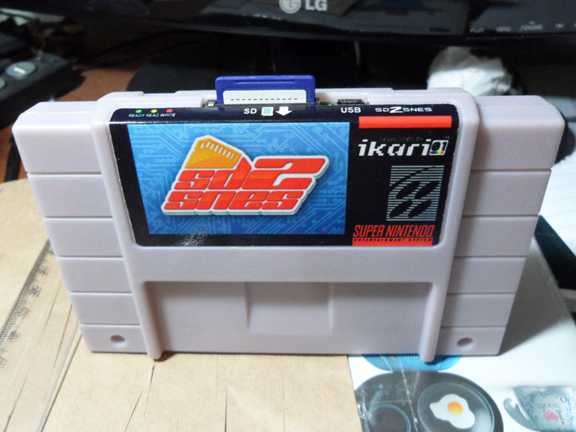
Thanks for the tips, Ramsis. I'd like to report that everything is in perfect working order. The PCB fits perfectly into the case (I was afraid it wouldn't, since the case belonged to a pirate Pikachu game, which is now homeless) and I just finished applying the label. It may not be perfect, but it looks fairly decent. Here's the finished cart:
Attachment:
 sd2snes-ready-1.jpg [ 131.72 KiB | Viewed 4875 times ]
Attachment:
 sd2snes-ready-2.jpg [ 141.43 KiB | Viewed 4875 times ]
Attachment:
 sd2snes-ready-3.jpg [ 114.18 KiB | Viewed 4875 times ]
I played with it a bit, but have to explore more!
I just paid the extra dough for the Stone Age Gamer deluxe edition.


While I definitely want the Super FX to be added, SA-1 would be great too. I really want to see more games using the MSU1.
MSU-1 is the most interesting part of the SD2SNES to me. It's a shame the PowerPAK doesn't seem to be capable of supporting it. =(
Greg2600 wrote:
I really want to see more games using the MSU1.
Me too. While adding anime FMVs to games (backports from later remakes, eg Chrono Trigger) is quite difficult, adding CD-audio is actually extremely simple. Takes about 30 minutes of effort per game. Filter out routine $214x accesses that always occur, and then spot the unique ones between songs playing. Jump up a few functions in the stack and there's your "lda #track; jsr loadAndPlayTrack", patch it with an MSU1 play track command, done. Brings in the possibility of adding orchestral / remix sound tracks to games and such.
byuu, are you going to release a MSU1 version of your translation of Der Langrisser, with cutscenes and the like from the PC-FX port?
Eventually I'll post an MSU1 patch to support the Langrisser II soundtrack (it's absolutely amazing, by the way.)
But no to the cutscenes. There's no source for high-quality encodings of any of them, and each game changes the story around a bit, and mixes them in with dialogue scenes and such. Far too much effort.
(In reply to a question in the
PowerPak thread ...)
marvelus10 wrote:
Have you considered working on the SD2SNES as well, maybe helping to implement some of the remaining chips?
Thanks, marvelus10.
Funny that you ask, because I fiddled around with the SD2SNES source a few months ago, and actually came up with a new menu design just for my own pleasure. But even though ikari_01 approved my efforts and asked me to help with a theme selector, I haven't had the time for that so far.
As far as the special chips are concerned: To be honest, I'm not proficient and confident enough in SNES programming (yet) to offer my help with that.
Anyway, here's what I did back in April:
Download:
menu_WIP06b.bin (Usage: Just replace menu.bin on your SD card with this file. Source code used was v0.1.5.)
Now you brought that up I do remember reading about it a while back. A custom menu screen option would be pretty nice, however when I got my SD2SNES I made a label to match the menu screen, I like that graffiti style of artwork.
Thank you for the answer, I look forward to more of your projects.
Ramsis wrote:
(In reply to a question in the
PowerPak thread ...)
As far as the special chips are concerned: To be honest, I'm not proficient and confident enough in SNES programming (yet) to offer my help with that.
SNES programming isn't really of any use at all in terms of implementing the enhancement chips. That's all Verilog/VHDL, which is an entirely different beast altogether.
qwertymodo wrote:
SNES programming isn't really of any use at all in terms of implementing the enhancement chips.
I don't fully agree. While
implementing a custom chip e.g. on an FPGA might indeed be a matter of being able to program your custom hardware, accurately
replicating the chip's behavior still requires you to understand its inner workings, its ports/registers, how it communicates with the SNES etc. In fact, I believe this is the hardest part of it all.
That's a big part of it, sure, but the hardest part is internal timings, some of which aren't even fully known yet.
So where can I buy the latest hardware version of this? stoneagegamer is all out of stock and the one on retrogate looks different. i'm confused what to buy...?
jwdonal wrote:
So where can I buy the latest hardware version of this? stoneagegamer is all out of stock and the one on retrogate looks different. i'm confused what to buy...?
I bought mine from Retrogate, easy purchase, fast delivery, no issues. krikzz (retrogate) was helping ikari with building the SD2SNES when the demand got to be too much before other resellers started selling them.
For those interested ikari_1 has invited people to create their own patches for the SD2SNES cart.
https://github.com/mrehkopf/sd2snes
Since this thread just got bumped, I thought I might as well add that this flash cart has been awesome to use. I just got it a couple weeks ago and it's been great for working with my SNES on my logic analyzer and uploading test ROMs for the SPC700. And of course...for playing games.
It may be expensive, but worth every penny.
I'll second that and give the thread another bump.
The SD2SNES is very impressive and I am learning how to use the MSU1 in my first ever homebrew game.


