I have an original US SNES that when you turn it on you just get a black screen. I have a post on this forum http://www.eevblog.com/forum/repair/sne ... t-startup/ of what I have tried so far to get it to work. They did suggest to post over here for more help so that is what I am doing. The tools I have to try and fix this are a multimeter, a Tektronix 465 100Mhz 2 channel scope and a HP 1661C logic analyzer with 3 pods (so 48 usable channels). Do you have any idea why the SNES does not start up the same way each time (at least according to the logic analyzer)?
It sounds like you've already:
* ensured that the CIC isn't getting in the way, so I assume that the /RESET pin on the cartridge edge is high, and the address bus is counting...
* ensured that (when present) the cartridge connector is making good contact.
It is possible for the SNES CPU to run code without the PPUs present, but you'll need a special program to do specific things given that there's no output methods available.
Do the controller parts do the (in-silicon) auto-read?
Are any of the parts getting noticeably warmer than other ones?
Unfortunately, where-as on the NES the different failures produce noticeably different symptoms, almost all failure modes produce the same black screen on the SNES.
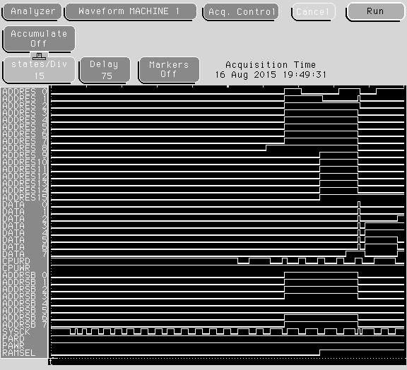
How would I check that the controller ports do the auto read and how would I check for that? Other then the regulator nothing appears to get very warm or much warmer then other components. I have attached a startup sequence that I captured with the logic analyzer. I can't remember if the cart was in the SNES or not in this capture (I think I was trying to get repeatable startups so there may have not been a cart in the SNES). I have labeled all of the pins that I was probing. You can open the file with any ASCII compatible reader. I do find it somewhat weird that the IRQ line never changes.
http://wiki.superfamicom.org/snes/show/ ... nd+Pinouts
If the controller daughterboard were plugged in, you'd check to see if LATCH pulsed high at 60 Hz and for each then CLOCK pulsed sixteen times (at about 1MHz). This is done entirely in silicon, so it's only a very minimal test that the CPU die works.
These pins are directly connected to the CPU, ultimately, so you could use jwdonal's redrawn schematics to find where to tap the signals, also.
Looking at the first couple hundred lines of the trace you have, it looks perfectly plausible:
- reads from 100, 1FF, 1FE because power-on-reset is the same sequence as an interrupt
- reads from the power-on vector at FFFC, FFFD
- power-on vector points to $8000
- execution continues logically thereafter.
Ok I have done the controler test and here is what I have found, the latch line stays low and all of the other signals on the controler port stay high. I have also reconected the resistor that I removed to disable the ppu chips. I have also reconected the CIC chip just incase there was some fault with it (there was no change the reset line was still high). The test results were the same with and without the cart. Does this mean there is something wrong with the CPU? Edit: I just tested this configuration on the logic analyzer and now I am not getting any data or garbage data (I don't think 0x50AA is a valid address) that loops.
Oh, no, I misunderstood: http://problemkaputt.de/fullsnes.htm#sn ... ticreading says that the software has to opt in first.
So whatever's going wrong is more complex than that :/
So whatever's going wrong is more complex than that :/
I agree that $50AA is not an address where things should be poking; there's nothing there in banks $00-$3F or $80-$BF.
Looking at the LA trace you have from before, it looks like it's waiting forever polling something ... it just executes from $8034 to $8049 over and over. (What game were you testing with?)
Looking at the LA trace you have from before, it looks like it's waiting forever polling something ... it just executes from $8034 to $8049 over and over. (What game were you testing with?)
I was testing with Super Mario World. I also have Super Mario Kart, Super Mario All Stars and Super Mario All Stars Super Mario World. The Super Mario World game is what gave me the most success when I first got the SNES so I stuck with it. I do want to make a test cart with a flash rom so that I can try to activate the minimal set of chips in the SNES to prove it is somewhat working (eg just video or just audio or just controler ports) if that is possible. I currently have the 2Mb flash chip programed with a video test but am unsure as to which crappy cart to get to mod into a flash cart.
Ah. In SMW, the loop from $008034 to $008049 is filling memory at $7F8002)... so the LA doesn't show anything there.
As far as I can tell, it looks like the CPU is ok, but who knows about the RAM or PPU...
As far as I can tell, it looks like the CPU is ok, but who knows about the RAM or PPU...
Ok, I have reattached all reset lines and have re disabled the CIC chip and have rerun the LA again and have attached the output. Listing is with out the cart in the SNES and Listing1 is with the cart in the SNES. Both of these readings had to be done by turning the SNES on and then selecting the RUN button on the LA otherwise I would just capture all zeros by arming the LA and then turning on the SNES. I am grabbing the trigger signal from the xin clock on the SNES.
In attachment #3690 ("LISTING1.txt") is waiting (forever?) while it hopes to upload data to the sound coprocessor.
In attachment #3689 ("LISTING.txt"), there's something weirder ... looks like something's repeatedly triggering the IRQ (writes to the stack at 01xx, followed by reads from FFFE and FFFF) and fetching garbage for the IRQ address.
In attachment #3689 ("LISTING.txt"), there's something weirder ... looks like something's repeatedly triggering the IRQ (writes to the stack at 01xx, followed by reads from FFFE and FFFF) and fetching garbage for the IRQ address.
I have tested the sound module in a working SNES and it works so I assume that there may be a bad connection to the sound module? What other signals in the SNES should I probe? The B address bus? Or some more signals from the sound module? It kind of makes sense now that when I would bend the cart in a certain direction (when the SNES was still mostly together) that I could get a random sound effect to play and usually repeat with a garbled screen. I will try to test all of the sound module pins tomorrow and get back to you. I still do not like the IRQ line staying high when I have a cart in the SNES but that could be due to it crashing so early on in the boot stage.
Bad connections to the sound module would be an obvious thing to test...
Unfortunately, I'm beginning to run out of ideas for things to try without a flashable cart. E.g. trying something that didn't use the PPU or APU would be the next obvious test...
Does anything ever produce anything visible at all?
You could test random signals on the PPU... but I fear that there wouldn't be any PPU bus activity if the CPU never enables it.
Well I found a broken /PAWR line going to the APU so I repaired that and the LA is still going through 0x2140 to 0x2144 address range and looping. I have noticed that the SNES now seems to be starting up in a consistent state so I think that is good. How I tested the connections to the APU was setting my meter in diode mode and looking for the protection diodes or transistors in the other chips. I am not sure if this is the right way to do it but it is fast. The SNES does not seem to change behavior when I pull the sound module. I have also attached a LA trace with triggering off the SYSCK to avoid the all zeros problem at power on.
Lately I've been repairing a bunch of Nintendo Super System PCBs (basically an arcade SNES), and have come across a LOT of "Black Screen" problems. Unfortunately, the majority of them have been bad CPUs.  To get CPUs to fix them, I have to pull them from SNES systems (I try to take from dead or heavily damaged systems)... some of them have also had bad CPUs though.
I'd recommend making a cartridge of the burn-in test cart ( https://tcrf.net/SNES_Burn-In_Test_Cart ). Getting the menu to boot must be fairly simple, because it'll boot even on a lot of bad CPUs (which then typically lock up after selecting a test, or fail one or more tests in the Burn-In Test). Unfortunately, if you find out that your CPU is bad, the only way to get a replacement is from another SNES... and it's a 100 pin QFP, so replacing it requires more than the typical repair tools/skills.
DogP
Well I have tried another of my cartridges (Super Mario All-Stars) and here is the result of the video output and reset glitching: https://youtu.be/dT9o6S2DnrU I was also able to get blue scrolling flashing bars and other random garbage as well that I did not film.
Looks like the PPUs and CPU at least partly work... weird that it's full of garbage, though. If you can get your hands on the SuperNES Test Program, maybe that'd be helpful...
I will try to find a crappy SNES cart to turn into a flash cart and put that program on it. I have attached a LA trace from when the SNES was doing the garbage video output. I suspect that the sound module (that the CPU seems to fail to get a response from) is causing it to crash in such a way as to leave weird stuff in the video ram. I know the sound module works fine because I have tested it in another working SNES.
... Why does /CPURD never go low in that most recent trace? /ROMSEL is flapping, but the actual control lines aren't...
I am starting to think that it is very broken. Is it possible that the CPURD and CPURW lines transition faster then the SYSCK line preventing my LA from picking them up? I have attached the LA trace from when it does the garbage colored blocks that you see in the video. I am starting to suspect that one of the chips is in latchup on the outputs or inputs.
That's definitely nonsense. Not only is /CPURD never moving, but the values on the address and data busses are changing wildly ... like it's just picking up (and maybe amplifying?) noise.
You have a point there. I will try to isolate the CPU and RAM and try to figure out what chip is causing this. I don't know if this idea would work but could I use a Arduino and some shift registers to simulate the CPU and try to get the PPU chips to do something? Or would this not work due to the clock signals as well as other signals that I would not be able to easily replicate with this setup? I was thinking of just controlling the address and data lines with the setup and holding the SNES CPU in reset.
If you have the skills/tools to desolder the CPU, or at least can keep its outputs tristated, that should work fine.
The PPU's interface to the CPU should be something you can improvise some simple test with an Arduino program fairly easily.
The PPU's interface to the CPU should be something you can improvise some simple test with an Arduino program fairly easily.
I have found an interesting discovery in that if I disconnect resistor R74 that allows the PPU to reset the CPU, cart and sound module and trigger my LA off the XIN clock instead of the SYSCK I get the CPURD and CPUWR lines to show up again. The heading SYSCK1 in the attached LA traces is actually SYSCK on the SNES. In the first trace the PPUs are not in reset and in the second one they are. The tests were done with the Super Mario All-Stars cart and the sound module installed. Also I have just realized that the PPUs have just a 8bit address bus and a 8bit data bus as well as a read and write control lines as well as HBLANK, VBLANK, and EXTLATCH. I am wondering how I would convert the 0x2100 to 0x213f registers into a 8bit value that the PPUs would understand? I think these are the values that the CPU is expecting on the address "A" bus but what comes out on the "PA" bus? Would I be correct in thinking that the "B" address bus is what is labeled in the color SNES schematic as CA16 to CA23? Also can I ignore the HBLANK, VBLANK, and EXTLATCH on PPU2 for now? I know some Arduino programming and would be able to probably get this to work if I could figure out what hex or binary values I would need to send to the PPUs for them to work. I am more of a hardware kind of guy not a software one but will learn the software bit if I have to. Also I am a beginner at SNES programing so I am sorry if some of my questions come across as stupid. I am also still learning how to best use my LA as well as I have only been using it for a few weeks and have had no formal training on how to properly use one (except from what I read from the users manual that was somewhat hard to understand).
I am sorry that I do not have much to add to this conversation, other than I've really run into a wall trying to fix broken Super Nintendo consoles. I have had a ton of luck with old NES consoles, but SNES... no luck.
I get the same problem as you: black screen of death. The system powers up just fine. I have replaced all caps, same thing. Switched around sound cards and other pieces from working systems, and nothing has helped.
I will follow this conversation. I really hope to solve this problem... I have thrown away quite a few boards in frustration due to not being able to fix them. I still have a couple that I have hope for though...
Good luck.
Poot36 wrote:
I am wondering how I would convert the 0x2100 to 0x213f registers into a 8bit value that the PPUs would understand? I think these are the values that the CPU is expecting on the address "A" bus
I think the PPUs are on the B/PA bus, so AFAIK you should just be able to use /PARD and /PAWR with PA0..PA7 and D0..D7.Hopefully someone will speak up if I've confused things.
Quote:
but what comes out on the "PA" bus?
The SNES is a little weird in that it has two address-and-control busses and only one data bus, but arguably that makes sense because the DMA controller only allows transfers between the two different address busses, allowing one cycle per byte (in contrast to the NES's DMA taking two cycles per byte).Quote:
Would I be correct in thinking that the "B" address bus is what is labeled in the color SNES schematic as A16 to A17?
I don't even see A16 and A17 on the SNES schematic, except for as part of "CA16" and "CA17" or where those signals connect to the SNES's DRAM and cartridge connector.Quote:
Also can I ignore the HBLANK, VBLANK, and EXTLATCH on PPU2 for now?
Should be safe.Quote:
if I could figure out what hex or binary values I would need to send to the PPUs for them to work.
I regret to say that I have never written any SNES programs at all, but maybe tepples's controller test program is a good enough starting point?Quote:
I am more of a hardware kind of guy not a software one but will learn the software bit if I have to. Also I am a beginner at SNES programing so I am sorry if some of my questions come across as stupid. I am also still learning how to best use my LA as well as I have only been using it for a few weeks and have had no formal training on how to properly use one (except from what I read from the users manual that was somewhat hard to understand).
Stop selling yourself short, you're doing fine.Now, as far as the LA traces go ... I dunno, I don't see anything obviously useful or anti-useful there.
I just realized that I goofed on my previous post in that it mentions address lines A16 and A17 when in reality it should be CA16 to CA23. Whoops! I think some older cartridge pinouts refer to those address lines as address B and that is what confused me. Will take a look at the controller test program and also capture what is being sent to the PPUs when I get that blocky flashy screen so that I can try to replicate that. I am just not sure if the Arduino is going to be fast enough or if the speed of the data going in doesn't mater as long as it is correct and is in the VRAM.
Poot36 wrote:
I just realized that I goofed on my previous post in that it mentions address lines A16 and A17 when in reality it should be CA16 to CA23.
Oh, yeah. Sometimes the 65816 documentation refers to the upper 8 bits of the address as the "bank", or B. Just to be even more confusing.Quote:
I am just not sure if the Arduino is going to be fast enough or if the speed of the data going in doesn't mater as long as it is correct and is in the VRAM.
The speed shouldn't matter, because I believe the PPU has a classic asynchronous interface, like ISA cards or static RAMs.Ok, I have finished wiring up my LA to the B address bus as well as some other pins. I have attached the trace and also two pictures of what each line is doing just after startup. I have noticed that address line 8 always starts a little earlier then the rest and that there seems to be some funniness with the sysck line (very short high burst) that also affects other lines as well. Also let me know if the .tif based pictures work or not.
I can view TIFs, but my browser won't display them in-line. They're also uncompressed, so it's better to convert them to something lossless and small like gif or png.
I already converted these two, and for no good reason I though it would be funny/useful to combine the images, so:
ADDRESS8+9.PNG [ 3.94 KiB | Viewed 2442 times ]
... Man, that looks familiar. I think I used this LA in college?
Anyway, regarding what I see in the LA trace ... it looks like the DMA controller is good?
[420C] ← 00, disabling all HDMA
[420B] ← 00, disabling all GP DMA
[2181] ← 00 \ (edit: typoed here)
[2182] ← 00 \
[2183] ← 7F ----- indirect WRAM pointer at $7F0000
[4300] ← 00, (A to PA, d/c, d/c, 2:A-inc, 3:always write to one address on PA bus)
[4301] ← 80, PA address
[4302] ← 02, \
[4303] ← 02, \
[4304] ← 04, --- start from address $040202
[4305] ← 00, \
[4306] ← 00, --- transfer 64KiB
[420B] ← 01, initiate DMA transfer set up in channel 1.
I'm really not clear what the code here is trying to do. There's ... nothing obviously useful about those memory locations. And you can't DMA transfer from RAM (as at $040202) to RAM (via PA $80). And the only value appearing on the data bus during the entire transfer is $B7, so ... uh...?
Is this still All-Stars?
Anyway, can you configure the LA to capture on a rising edge of SYSCK? It should help stretch out the 8192-sample recording limit. ... although not enough, if something does another 64K-long DMA transfer like this.
I already converted these two, and for no good reason I though it would be funny/useful to combine the images, so:
Attachment:
ADDRESS8+9.PNG [ 3.94 KiB | Viewed 2442 times ]
Anyway, regarding what I see in the LA trace ... it looks like the DMA controller is good?
[420C] ← 00, disabling all HDMA
[420B] ← 00, disabling all GP DMA
[2181] ← 00 \ (edit: typoed here)
[2182] ← 00 \
[2183] ← 7F ----- indirect WRAM pointer at $7F0000
[4300] ← 00, (A to PA, d/c, d/c, 2:A-inc, 3:always write to one address on PA bus)
[4301] ← 80, PA address
[4302] ← 02, \
[4303] ← 02, \
[4304] ← 04, --- start from address $040202
[4305] ← 00, \
[4306] ← 00, --- transfer 64KiB
[420B] ← 01, initiate DMA transfer set up in channel 1.
I'm really not clear what the code here is trying to do. There's ... nothing obviously useful about those memory locations. And you can't DMA transfer from RAM (as at $040202) to RAM (via PA $80). And the only value appearing on the data bus during the entire transfer is $B7, so ... uh...?
Is this still All-Stars?
Anyway, can you configure the LA to capture on a rising edge of SYSCK? It should help stretch out the 8192-sample recording limit. ... although not enough, if something does another 64K-long DMA transfer like this.
The game is still All-Stars. The SNES has the the resistor from the reset line that comes out of PPU2 that holdes the CPU, RAM and sound module in reset disconnected (I think it is R72 or R74). I can trigger off the sysck line and I think I can trigger off a data pattern but I will need to read my LA manual to figure out how to do it. I will loose the CPURD and CPUWR signals by doing this though (trigger off SYSCK). The LA is a HP 1661C if you are wondering. I will try to convert the tif files to jpeg in the future. Sorry about that. It also looks like the SNES is trying to enable the display but ends up turning it off as well as trying to initialize the sound module.
Poot36 wrote:
I will loose the CPURD and CPUWR signals by doing this though (trigger off SYSCK).
Oh? Eh, not worth it, then – basically the useful thing to know is the value of the various busses on a rising edge of any of CPURD, CPUWR, PARD, PAWR.Quote:
I will try to convert the tif files to jpeg in the future. Sorry about that.
Wait, wait, NOT jpeg. Almost anything but jpeg. JPEG does great for photographic pictures with soft gentle brightness ramps in it, but badly for 6-grey images like these.Also, it's not like saving 200kB is really worth that much. Don't feel bad about it.
---
Anyway, if I compare what the LA trace is doing to what the game "ought" to be doing (according to NO$SNS's debugger), I actually see some useful things:
At $00866D, SMAS has the following code:
Code:
sta $2181
sty $2183
lda #$8000
sta $4300
lda $02
sta $4302
ldy $04
sty $4304
lda $00
sta $4305
ldy #1
sty $420B
In the debugger, when this routine is first called, the first five bytes of memory are $00 $04 $00 $FC $07—it should be trying to transfer $0400 bytes from address $07FC00, and instead it's getting open-bus values.sty $2183
lda #$8000
sta $4300
lda $02
sta $4302
ldy $04
sty $4304
lda $00
sta $4305
ldy #1
sty $420B
Oh, right. You said you disabled the RAM. Well, it definitely shows that.
In this trace, SYSCK itself looks interesting. It's not 50/50 duty; slow cycles seem to have it high longer while CPURD is low longer. This confirms my suspicion about 3/5 ratios. There are also what appear to be a few very short pulses on SYSCK; what do those signify?
PNG would be far better.
Poot36 wrote:
I will try to convert the tif files to jpeg in the future.
PNG would be far better.
Here's a plot of just the control signals: http://eamp.org/li/controlsignals8.png (2kB, Warning: 16400 × 64 pixels) Each input sample was converted into two horizontal pixels (to allow the vertical transitions to not obscure the end value)
The short pulses might be glitches? The entire thing appears to be using the 21.5MHz SNES master clock for the sample clock.
The short pulses might be glitches? The entire thing appears to be using the 21.5MHz SNES master clock for the sample clock.
Ok, I have converted the pictures to .png. I have found out that triggering on SYSCK is a bad idea because you do end up loosing the CPURD, CPUWR, PARD, and PAWR lines and sometimes the LA will stop capturing if it does not see a clock for a predetermined time. I have captured a trace by leaving the SNES running but just re-triggering the LA. The RAM chip is still being reset, all I have done is prevented the PPU2 chip from holding it (and the CPU and Sound Module) in reset by disconnecting R74 in the schematic. This is the /RESOUT1 line. The CPU still pulls this reset line high.
Unfortunately, this trace just shows garbage again :/
Code:
time db addr /rd /wr pa /pard /pawr /ram +refresh
7795 FE<-[000D] 0 1 03 1 1 1 0
7801 3C<-[000E] 0 1 03 1 1 1 0
7809 7C<-[001F] 0 1 04 1 1 1 0
7816 00<-[3E1A] 0 1 06 1 1 1 0
7823 FC<-[01FF] 0 1 04 1 1 1 0
7827 18<-[0011] 0 1 04 1 1 1 0
7837 00->[7EE8] 1 0 CA 1 1 1 0
7844 13->[7EE7] 1 0 C9 1 1 1 0
7851 39<-[77FF] 0 1 C4 1 1 1 0
7863 00<-[3933] 0 1 0D 1 1 1 0
7867 00<-[3935] 0 1 0D 1 1 1 0
7875 0C<-[C3FF] 0 1 00 1 1 1 0
7881 4B<-[0001] 0 1 00 1 1 1 0
7885 0A<-[0001] 0 1 00 1 1 1 0
7893 D7<-[8A42] 0 1 02 1 1 1 0
7903 D7->[8A4B] 1 0 42 1 1 1 0
7909 C1<-[8A4B] 0 1 40 1 1 1 0
7915 08<-[0003] 0 1 01 1 1 1 0
7921 47<-[0004] 0 1 01 1 1 1 0
7927 06<-[0005] 0 1 01 1 1 1 0
Those aren't sensible addresses to be reading from or writing to.7795 FE<-[000D] 0 1 03 1 1 1 0
7801 3C<-[000E] 0 1 03 1 1 1 0
7809 7C<-[001F] 0 1 04 1 1 1 0
7816 00<-[3E1A] 0 1 06 1 1 1 0
7823 FC<-[01FF] 0 1 04 1 1 1 0
7827 18<-[0011] 0 1 04 1 1 1 0
7837 00->[7EE8] 1 0 CA 1 1 1 0
7844 13->[7EE7] 1 0 C9 1 1 1 0
7851 39<-[77FF] 0 1 C4 1 1 1 0
7863 00<-[3933] 0 1 0D 1 1 1 0
7867 00<-[3935] 0 1 0D 1 1 1 0
7875 0C<-[C3FF] 0 1 00 1 1 1 0
7881 4B<-[0001] 0 1 00 1 1 1 0
7885 0A<-[0001] 0 1 00 1 1 1 0
7893 D7<-[8A42] 0 1 02 1 1 1 0
7903 D7->[8A4B] 1 0 42 1 1 1 0
7909 C1<-[8A4B] 0 1 40 1 1 1 0
7915 08<-[0003] 0 1 01 1 1 1 0
7921 47<-[0004] 0 1 01 1 1 1 0
7927 06<-[0005] 0 1 01 1 1 1 0
Hmm, I wonder if the SNES has crashed after attempting to execute some corrupted code. Would a bad RAM chip cause this or is it most likely the CPU? If I disconnect the RAM chip (eg keep it in reset or use the chip select line to disable it) what should I expect the CPU to do? Is there a off the shelf RAM chip that I could try replacing it with?
Really hard to tell, either could be breaking things. For all I know, SMAS could just start executing random crud if any peripheral isn't working.
(e.g. There's the known bug in the revision 1 CPU's DMA controller (revision is indicated on top of the CPU package, 5A22-nn); if SMAS is writing specific wrong garbages to the DMA controller, because it expected valid values in RAM ... well, we don't actually know what that crash looks like, in an electrical sense.)
Anyway, what's keeping you from making a test cart? Lack of PROMs? Lack of programmer? You're quite clearly already very good with a soldering iron...
I got a 2Mb 120ns eeprom that I think will work and have programmed it on a 1988 Data I/O using the site 48 plugin. It has two 720Kb floppy drives and has boot software from you will never believe this 2006 running on it! It uses a serial port for communication and takes 5 minutes or so to start up off the floppy drive (old slow 10Mhz Motorola based processer I think). I am still trying to find a cart to modify and I don't look forward to removing the existing rom chip without damaging it. I think you are right that I am just making things more complicated then they need to be with a standard cart. What cart should I be looking for to run the test programs that have been mentioned in previous posts? I think it has to be a LoROM cart.
Is this an UVEPROM or EEPROM? A lot of the earlier SNES carts are DIP; the later ones tend to be SMT. For reference, you can look at the pages on snescentral.com.
Alternatively, if you have the ability to get a PCB made (such as a PCB mill), I have a very simple design that would accept a 128 to 512 KiB EEPROM like the SST39SF0x0 series. It's basically identical to the 1A0N and 1JON official PCBs.
Alternatively, if you have the ability to get a PCB made (such as a PCB mill), I have a very simple design that would accept a 128 to 512 KiB EEPROM like the SST39SF0x0 series. It's basically identical to the 1A0N and 1JON official PCBs.
Hi. I'm new here. I own a used game store and have several SNES consoles with the same problem. In my many repair attempts I did notice one strange occurrence. A "Jeopardy" game cartridge I used for testing would actually load (briefly) on these consoles. Only for a few seconds, but the title screen would be visible. No other cartridge I used would do this. Not sure if this means anything. Just thought I would throw it out there.
Ok, I have finally got a cart to make into a test cart (Donkey Kong Country) that had a damaged ROM chip. I have attached a socket and have preformed the 2 pin swap but only connected the CS line due to my chip only having 2mb (256Kb) of space on it. I have used the snesROMUtil to byte swap the .sfc file and programmed it to the chip however it is not working. The flash chip is a AS29F2008-12 made by ASD and I can not find a datasheet for it and my programmer does not have it listed so I selected Winbond W29C020 in my programmer instead. The cart is labled SHVC-1J1M-11 and has a MAD-1 chip on it. Am I doing this wrong or do I need a 27c801 for this utility to work? Is there a more compatible flash chip that I can select in my programmer? The original ROM chip does have a small crack like blister showing on the package, is it possible that it damaged other chips on the board when it died? Should I bypass the MAD-1 chip?
Quote:
but only connected the CS line
I hope that that means that both the PROM's /OE and /CE pins are connected now?Quote:
and programmed it to the chip however it is not working.
Ok, what are you testing with? The smaller the better, because it reduces the number of possibilities for things to screw up.Also, I hope you have a known-good SNES to distinguish between "cart" and "console" ?
Quote:
The flash chip is a AS29F2008-12 made by ASD and I can not find a datasheet for it and my programmer does not have it listed so I selected Winbond W29C020 in my programmer instead.
If you remove power to the 'PROM, restore power, and the programmer verifies, you can assume it worked.Poot36 wrote:
(Donkey Kong Country) [...] The cart is labled SHVC-1J1M-11 and has a MAD-1 chip on it.
Ok, I'm looking at 1J1M for reference.Quote:
Am I doing this wrong or do I need a 27c801 for this utility to work?
No, but you'll need to pad and then truncate off duplicates: see this bug report for SNES ROM Utility.Alternatively, why do you (think you) need to endian-swap the bits?
Quote:
Is there a more compatible flash chip that I can select in my programmer?
No idea, unfortunately. I can't even find out who "ASD" was.Quote:
The original ROM chip does have a small crack like blister showing on the package, is it possible that it damaged other chips on the board when it died? Should I bypass the MAD-1 chip?
Can't hurt. If you do do that, make sure you disable the RAM on the cart: the MAD-1 is basically a 74'139 (responsible for decoding RAM, or multiple ROMs) plus a battery backup protection circuit.I think I figured out a few things. First I meant OE not CS (was reading off the SNES schematic). Second I think the "J" letter printed on the cart label means that it is a HiROM cart and all of the ROMs that I am using are LoROM. Third the byte swap is so that I only have to change the positions of 2 pins of the EEPROM instead of 5 pins due to the nonstandard pin placement of the cart vs EEPROM. After reading the extra note of the utility my roms are only 2mb so from what I gather I need to expand it to 8mb and then run it through the utility but could I then shrink it back to 2mb and have it still work is the big question? Forth is there a way to convert the LoROM file to a HiROM one or will I have to modify the cart further? Fifth I do have a working SNES and can confirm that the cart's CIC (lockout) chip is still functioning. I have programed this chip before (but only as a 1mb chip by holding the last address line permanently low and selecting the W29C010 from the programers list) for a 486 motherboard and it worked but would sometimes give me errors I think due to the board been flaky or it somehow rewriteing the chip (it was designed for a UV EPROM). I think the second problem is the root cause of this not working. Oh well at least I am learning and no magic smoke has come out yet.
Poot36 wrote:
is there a way to convert the LoROM file to a HiROM one or will I have to modify the cart further?
Yes, but you lose half the capacity.HiROM can store LoROM by taking each successive 32KiB of the input file and putting it twice, sequentially, in the output file. (i.e. ABCDEFGH becomes AABBCCDDEEFFGGHH).
It's probably easier if you find one of the various tiny SNES tests, like the pile of 32 KiB homebrew that have been made over the years... not that I can find an obvious listing of these.
If nothing else, I took tepples's spadtest-0.01 and reassembled it to be eensy (just 8KiB). Duplicate it to fill your 'PROM.
The patch containing the source differences to make it 8KiB instead of 256KiB is included in the zip.
I have figured out that I had miswired the OE line (it was connected to A22 on the cart). I have fixed that and rewired the EEPROM socket so that I do not have to use the swapbin utility that apparently does not work with files smaller then 8mb even if you extend the file to that size. I have tried the 8Kb file and copy pasted it to 256Kb and all I get is a black screen but I do get video synchronization pulses. I think trying to find a HiROM game or demo that is 256Kb would be my best bet, do you know of any? Is there anything else I can try short of totally rewireing the cart for LoROM use?
The tiny 8KiB thing reaaaaally should work. Only the first 829 bytes and last 32 matter; the middle 7KiB are pictures and padding. So if it doesn't work, there's got to be a wiring or programming issue...
Anyway, any image that is 32KiB or smaller is a strict subset of both LoROM and HiROM, so that's definitely not the problem you're having.
So anyway, I guess there's a bunch of free-to-redistribute SNES images from zophar...
Anyway, any image that is 32KiB or smaller is a strict subset of both LoROM and HiROM, so that's definitely not the problem you're having.
So anyway, I guess there's a bunch of free-to-redistribute SNES images from zophar...
I have attached the 8K copy pasted file that made it 256K just in case I did some thing wrong with it (I used notepad by the way). Wold it be worth it testing these files in a emulator or would that no correctly simulate the SNES?
Yahhh! I fixed it! I used the copy binary function of Notepad++ instead of a Ctrl + A Ctrl + C Ctrl + V in just Windows notepad. I have attached the file that I used. I also tried the cart in the broken SNES and still got a blank screen . I also figured out that on one of my controllers the R trigger does not work.
Hm. Well, on the bright side, this test program is simple enough that we can pretty conclusively diagnose what's going on/wrong from a logic analyzer trace.
You should see mostly-sequential addresses in the range of $E000 through $E33D as it executes.
You should see mostly-sequential addresses in the range of $E000 through $E33D as it executes.
Poot36 wrote:
I have attached the 8K copy pasted file that made it 256K just in case I did some thing wrong with it (I used notepad by the way).
Text editors are generally very bad at keeping binary files intact. Notepad destroyed some of the data.
Have you ever heard of hex editors? They're much better for manipulating binary files. I like HxD, but there are many to choose from.
Under Windows, the idiomatic technique for "doubling up" a headerless ROM whose size is a power of 2 uses copy /b in the command prompt.
It won't work with headered ROMs, such as NES ROMs with an iNES or NES 2.0 header or Super NES ROMs with a copier header. For those, you have to separate out the PRG ROM (and in the NES's case, the CHR ROM) before doubling.
Code:
rem starting with a ROM 8192 bytes (64 kbit) in size:
copy /b rom_64kbit.sfc+rom_64kbit.sfc rom_128kbit.sfc
copy /b rom_128kbit.sfc+rom_128kbit.sfc rom_256kbit.sfc
copy /b rom_256kbit.sfc+rom_256kbit.sfc rom_512kbit.sfc
copy /b rom_512kbit.sfc+rom_512kbit.sfc rom_1Mbit.sfc
copy /b rom_1Mbit.sfc+rom_1Mbit.sfc rom_2Mbit.sfc
rem now the ROM is 262144 bytes (2 Mbit) in size
It won't work with headered ROMs, such as NES ROMs with an iNES or NES 2.0 header or Super NES ROMs with a copier header. For those, you have to separate out the PRG ROM (and in the NES's case, the CHR ROM) before doubling.
Well here is the LA trace. It appears to loose it around the 2.5K to 2.7K region. I am assuming that the video gets setup but does not receive any valid data after that so I just get a blank screen. I have reconnected the R74 resistor from the /resout line from PPU2 and have figured out how to trigger my LA on the first address that the SNES sends out (0x0100) so that I do not wind up with all zeros in the trace.
Hm. The last few instructions before it goes crazy are:
So ... why on earth is the stack pointer randomly dying and changing from 01FB to FFFF? I have no idea. Theoretically only the TCS and TXS instructions should be able to change the stack pointer, and neither are present.
So I have to guess you've got bogons in your CPU. It might be induced by power rail noise, but beyond that I don't have any ideas.
Code:
t dt addr r w pa r w m f
1975 22 E0C1 0 1 C0 1 1 1 0 - JSL $80E132
1983 32 E0C2 0 1 C0 1 1 1 0
1991 E1 E0C3 0 1 C0 1 1 1 0
1999 80 01FF 1 0 CF 1 1 0 0
2013 80 E0C4 0 1 C1 1 1 1 0
2021 E0 01FE 1 0 CF 1 1 0 0
2029 C4 01FD 1 0 CF 1 1 0 0
2037 8B E132 0 1 0C 1 1 1 0 - PHB
2052 00 01FC 1 0 CF 1 1 0 0
2060 4B E133 0 1 0C 1 1 1 0 - PHK
2074 80 01FB 1 0 CE 1 1 0 0 -- last time it correctly interacts with the stack in the normal place
2082 AB E134 0 1 0D 1 1 1 0 - PLB
2102 E0 FFFF 0 1 CF 1 1 1 0 -- that's not where the stack is... also the first time the cpu ever tries to read a value from the stack or RAM
2110 E2 E135 0 1 0D 1 1 1 0 - SEP #$20
2118 20 E136 0 1 0D 1 1 1 0
2132 9C E137 0 1 0D 1 1 1 0 - STZ $2121
2140 21 E138 0 1 0E 1 1 1 0
2148 21 E139 0 1 0E 1 1 1 0
2156 00 2121 1 0 08 1 1 1 0 -- /PAWR should have gone low, too... it doesn't because the PLB means that this address is treated as $E02121, not $002121
2164 C2 E13A 0 1 0E 1 1 1 0 - REP #$30
2172 30 E13B 0 1 0E 1 1 1 0
2186 A9 E13C 0 1 0F 1 1 1 0 - LDA #$2202
2194 02 E13D 0 1 0F 1 1 1 0
2202 22 E13E 0 1 0F 1 1 1 0
2210 A2 E13F 0 1 0F 1 1 1 0 - LDX #$F400
2218 00 E140 0 1 40 1 1 1 0
2226 F4 E141 0 1 40 1 1 1 0
2234 A0 E142 0 1 40 1 1 1 0 - LDY #$0008
2242 08 E143 0 1 40 1 1 1 0
2250 00 E144 0 1 41 1 1 1 0
2258 22 E145 0 1 41 1 1 1 0 - JSL $80E314
2266 14 E146 0 1 41 1 1 1 0
2274 E3 E147 0 1 41 1 1 1 0
2282 80 FFFF 1 0 CF 1 1 1 0 -- so why IS the stack wrong?
2296 80 E148 0 1 42 1 1 1 0
2304 E1 FFFE 1 0 CF 1 1 1 0
2312 48 FFFD 1 0 CF 1 1 1 0
2320 08 E314 0 1 05 1 1 1 0 - PHP
2334 05 FFFC 1 0 CF 1 1 1 0
2342 C2 E315 0 1 05 1 1 1 0 - REP #$30
2350 30 E316 0 1 05 1 1 1 0
2364 8D E317 0 1 05 1 1 1 0 - STA $4300
2372 00 E318 0 1 06 1 1 1 0
2380 43 E319 0 1 06 1 1 1 0
2388 02 4300 1 0 00 1 1 1 0
2396 22 4301 1 0 00 1 1 1 0
2404 8E E31A 0 1 06 1 1 1 0 - STX $4302
2412 02 E31B 0 1 06 1 1 1 0
2420 43 E31C 0 1 07 1 1 1 0
2428 00 4302 1 0 00 1 1 1 0
2436 F4 4303 1 0 00 1 1 1 0
2444 8C E31D 0 1 07 1 1 1 0 - STY $4305
2452 05 E31E 0 1 07 1 1 1 0
2460 43 E31F 0 1 07 1 1 1 0
2468 08 4305 1 0 01 1 1 1 0
2476 00 4306 1 0 01 1 1 1 0
2484 E2 E320 0 1 08 1 1 1 0 - SEP #$20
2492 20 E321 0 1 08 1 1 1 0
2506 8B E322 0 1 08 1 1 1 0 - PHB
2520 E0 FFFB 1 0 CE 1 1 1 0 -- stack is still wrong
2528 68 E323 0 1 08 1 1 1 0 - PLA
2548 E0 FFFB 0 1 CE 1 1 1 0 -- stack
2556 8D E324 0 1 09 1 1 1 0 - STA 4304
2564 04 E325 0 1 09 1 1 1 0
2572 43 E326 0 1 09 1 1 1 0
2580 E0 4304 1 0 01 1 1 1 0
2588 A9 E327 0 1 09 1 1 1 0 - LDA #1
2596 01 E328 0 1 0A 1 1 1 0
2604 8D E329 0 1 0A 1 1 1 0 - STA 420B
2612 0B E32A 0 1 0A 1 1 1 0
2620 42 E32B 0 1 0A 1 1 1 0
2628 01 420B 1 0 02 1 1 1 0
2636 28 E32C 0 1 0B 1 1 1 0 - PLP
2656 09 FFFC 0 1 CF 1 1 1 0
2664 6B E32D 0 1 0B 1 1 1 0 - RTL
2684 E0 FFFD 0 1 CF 1 1 1 0
2692 08 FFFE 0 1 CF 1 1 1 0
2700 E0 FFFF 0 1 CF 1 1 1 0 -- fetched return address is $E008E0
2708 00 08E1 0 1 C8 1 1 1 0 -- parsed as BRK #0
2716 00 08E2 0 1 C8 1 1 1 0
2724 E0 FFFF 1 0 CF 1 1 1 0 -- tries to push bogus return address
2732 08 FFFE 1 0 CF 1 1 1 0 -- (but's that's ROM)
2740 E3 FFFD 1 0 CF 1 1 1 0
2748 09 FFFC 1 0 CF 1 1 1 0
2756 08 FFE6 0 1 C9 1 1 1 0 -- correctly fetching BRK handler from FFE6
2764 E0 FFE7 0 1 C9 1 1 1 0
2772 40 E008 0 1 02 1 1 1 0 - RTI
2792 09 FFFC 0 1 CF 1 1 1 0 -- flags
2800 E0 FFFD 0 1 CF 1 1 1 0 -- parse vectors as return address
2808 08 FFFE 0 1 CF 1 1 1 0
2816 E0 FFFF 0 1 CF 1 1 1 0
2824 00 08E0 0 1 C8 1 1 1 0 -- so end up at the same wrong place
2832 00 08E1 0 1 C8 1 1 1 0
So ... why on earth is the stack pointer randomly dying and changing from 01FB to FFFF? I have no idea. Theoretically only the TCS and TXS instructions should be able to change the stack pointer, and neither are present.
So I have to guess you've got bogons in your CPU. It might be induced by power rail noise, but beyond that I don't have any ideas.
Well I have tried powering the SNES from a battery pack ~11.5V 0.377A was drawn when it was connected to the fuse in the SNES. Is this high current consumption for a SNES? I also have a LA trace from it running off battery and I don't think it will be very different (I still am having it not give me consistent readings on startup). I also tried 5V from 4 NiMH battery's bypassing the regulator and it drew around 0.300A or so (battery's were somewhat flat). I still got a black screen on all of the tests. Is it possible that there is some sort of big power consumption that happens when it goes bad that I would need a scope with a storage memory to capture? Do the SMD caps on the SNES usually go bad? I wonder if a test program under 2.5K or so would work or not. It would be nice if this http://wiki.superfamicom.org/snes/show/ ... ES+Program tutorial would be rewritten as small as possible and as a NTSC version. Would that be a good test?
As far as I know, that sounds like typical power consumption.
Electrolytics eventually dry out, but SMT ceramics should be fine. And I was hoping power rail coupling issues, rather than the wall wart producing bad power... although verifying that it's not the wall wart is useful.
It tentatively looks like any program that doesn't use the stack should be ok, at least for now. So ... here's a hacked together a version of tepples's test that doesn't use the stack at all... the bit where the 65816 doesn't support setting the DBR (A16..A23 during data accesses) except by using the PLB instruction is a lot inconvenient. But for an image that's at most 32 KiB in size, I guess it's trivial to work around (since the DBR powers on as 0)
Patch and sfc file are included. This change is (obviously) a lot more invasive than just changing the linking behavior, so the patch is a good deal larger.
Well good news it does boot and show the image and both controller ports work. However it usually takes a push of the reset switch to make it work. On first power application it will sometimes show a black screen or a screen with garbled lines, triangles or other nonsense and if I reset it after that it will start working properly and stay working. I have attached a LA traces of it booting to the black screen, after reset and when it is running. The reset trace was triggered off the SYSCK going high due to the address bus not sending the 0x0100 again but was still clocked of the XIN pin. I think this proves the PPUs are ok. Is it possible that one of the unused pins on the CPU is not being grounded or held high properly (internally in the CPU die or externally) and causing this weard condition? I have found that the longer the SNES is left in the working state the less likely that removing power and draining the caps will affect it starting up (ie it will start properly on first power up).
Edit: I think the glitching at first powerup may have been caused by a bad or dirty cartridge connection, will check this tomorrow.
Edit: I think the glitching at first powerup may have been caused by a bad or dirty cartridge connection, will check this tomorrow.
Poot36 wrote:
I think this proves the PPUs are ok.
It's not an exhaustive test—after all, it's just a single layer of background, with sprites, using SNES mode 0 (four layers of 2bpp graphics). But it does insinuate the only problem you're having is the CPU's stack.Poot36 wrote:
Is it possible that one of the unused pins on the CPU is not being grounded or held high properly (internally in the CPU die or externally) and causing this weird condition?
It's certainly possible that this could be caused by a cold solder joint or a broken bond wire, but I don't really have any ideas where to even guess. Especially without a decap'd 5A22 to look at where the stack pointer is on the die, or what's near it.We know that the RAM and DMA work, since the sprites show up in the right places and with the right tile.
Is there any other tests that I can do to try and figure out what else is broken? Is there any games out there that do not use the stack at all? Would it be worth it to pull up and test each of the extra pins on the CPU to see if any of them read differently on my meter? Does this test rule out power rail coupleing?
Without going and writing / rewriting some test for all of the PPU modes, it'd be hard to say conclusively. But really, I'd assume one single failure.
Unfortunately, the stack is such an intrinsic part of almost all CPUs that I can't imagine anything existing that doesn't use it. If nothing else, not having the stack means you can't even use interrupts.
It doesn't rule out power rail coupling because the symptom was the stack pointer being reset to FFFF when the PLB instruction executed. I suppose it's conceivable that the PLB instruction is actually the only problem... that sounds easy to test. Here's yet another version of tepples's pad test; this one ONLY omits PLA/PLB/PLK/PLP/PHA/PHB/PHK/PHP instructions, but still uses the stack in JSR/JSL/RTI/RTS/RTL instructions.
Well I can confirm that the glitching graphics that I was seeing with the first test program that ran was due to a bad cart connector connection. Also the new test works as well. I guess this is good but it is weird that the PLB instruction would cause it to crash. I have attached a LA trace of this working startup. Do you think running the SNES at a lower (1.79Mhz) or higher (3.58Mhz) speed would change its behavior?
I think that program is already a slow ROM (mode $20: high nibble means slow ROM, low nibble means LoROM). Someone could patch the init sequence to make it a fast ROM (mode $30) and see what breaks.
You actually already thought of that, tepples; it inspects its own header and adjusts the execution speed register according to the $10s bit at memory location $00FFD5.
To change any of the spadtest things I've sent to take advantage of this, use a hex editor to change the byte at address 0x1FD5 from 0x20 (" ") to 0x30 ("0").
----
On the other point: If it's just the PLB instruction, then I'd be surprised if there were anything you can fix externally.
The silver lining is that modifying other existing ROMs (to further validate that the PPUs work) becomes feasible. So ... here's a copy of nocash's Magic Floor where I removed the PLB instruction. It's still only mode 0.
Here's a modified copy of a, uh, certain group's intro. PPU mode 1.
And here's a modified random trippy mode 7 something:
To change any of the spadtest things I've sent to take advantage of this, use a hex editor to change the byte at address 0x1FD5 from 0x20 (" ") to 0x30 ("0").
----
On the other point: If it's just the PLB instruction, then I'd be surprised if there were anything you can fix externally.
The silver lining is that modifying other existing ROMs (to further validate that the PPUs work) becomes feasible. So ... here's a copy of nocash's Magic Floor where I removed the PLB instruction. It's still only mode 0.
Attachment:
—also tests the APU (yeah, I know you already removed the module).Here's a modified copy of a, uh, certain group's intro. PPU mode 1.
Attachment:
And here's a modified random trippy mode 7 something:
Attachment:
Well this is interesting, the Magic Floor appears to try to run but never does (screen flickers slightly over and over and will sometimes get graphical garbage on screen), the Anthrox demo is glitching video: https://youtu.be/HAledVusSGI it shows black and wight most of the time but color bars are present and when I press the Start button to view the credits they are shimmering as well (also have a problem having this one start up continually on power up), the mode 7 demo works great. All of these demos work properly on my working SNES so I think I can rule out the homebrew cart and rom file multiplying. Could I still have bad solder connections on some of the chips or cartridge connector or does the mode 7 demo rule that out? I will get a LA trace from the Maic Floor one tomorrow. I have also found out that the previous owner of this SNES was trying to see if it would work and tried to use a NES power adapter on the SNES using jumper wires (I assume they thought it would work due to the label on the bottom of the SNES mentioning a AC adapter). Would having AC from the NES adapter have damaged the SNES? In the schematic I see a diode as well as a 5V regulator that should prevent the AC from reaching the chips. I also know that the audio amp still works because I was originally getting some random audio out.
Do you have an oscilloscope as well as that LA? Could you check how clean the 21.5MHz clock output is?
It'd be nice to check both medium-term (ms range) stability as well as cycle-to-cycle jitter.
----
9VAC before the fuse and regulator shouldn't have harmed anything, although it might cause the filter caps to get hot and shorten their lives.
9VAC after the diode and fuse but before the regulator probably permanently damaged the electrolytics on the input stage. ... and possibly could have damaged Q18 (the NPN on the input stage for the semi-regulated higher-voltage supply)... maybe?
I can check the 21.5Mhz clock but you won't see a square wave due to my scope only having a 100Mhz bandwidth (a Tektronix 465).
Fortunately, sharpness of the transition doesn't really matter here.
The NES power adapter was connected to the barrel jack on the outside of the SNES so I am going to assume that it would have been ok. I will take a look at the XIN signal with my scope and see if there is any of the problems you mentioned. Got any ideas why the Anthrix intro demo would corrupt like that? It looks like it is trying but failing on correctly displaying the colored ball text (not sure you can make this out in the video, if you want I can try to use my Huppage 1600 TV tuner capture card but I have no clue as how to reduce the bit rate so I do not wind up with a very large file to upload). Stupid 512kbits/s upload speed should be 1mbits/s. 
NTSC console, right?
If the 21.5MHz master crystal is significantly changing frequency, the TV's chroma killer will activate, producing a monochrome signal. This is consistent with the scanlines being very jittery like what I saw, also.
The easiest ways to check for jitter or drift is to set an edge trigger and set the horizontal position a few cycles later (for jitter) or many cycles later (ten thousand or so, about 1ms, for drift).
If it is significantly changing frequency, I'd strongly suspect misregulation of the +5V rail; try putting another 'scope probe on +5V and looking for noise there.
You could also check PPU2 pin 3, which is master clock ÷ 6. (The division will mask jitter some, but it might be helpful anyway)
I was able to see what you were talking about in the youtube video, so I don't think you need any more sophisticated capture stuff yet. But I'd assume a single field (or maybe a few sequential ones) would be sufficient, should the need arise.
Poot36 wrote:
Stupid 512Kbps upload speed should be 1Mbps.
My downstream is like 10mbit/s. My upstream is like 200kbit/sec. I don't think that I can do all those things that you just mentioned on my 1970s purely analog scope. The mode 7 and controlle test colors are sold but maybe they work differently then this test. I am using the S-Video input on my Sony PVM series studio broadcast monitor so I would like to think it would have a more robust color sync circuit. I think I screwed up the units, my download speed is around 6mbits/s so I guess that is the trade off (it is a ADSL line and according to the modem the maximum upload speed that the line can support is a few kbits/s above 1mbits/s so I think that if I removed the dialup modem (used for scan to fax on the computer) that is in parallel with it the speed may go back up (using the telephone out on the dialup modem to go to the ADSL modem).
I could have sworn I could check for jitter on the tube-based Tek 547 ...
Anyway, in the manual for the 465, it talks about "Delayed Sweep Displays", which should be the right thing for this.
Anyway, in the manual for the 465, it talks about "Delayed Sweep Displays", which should be the right thing for this.
Well I just looked at both signals on my scope and they look solid (used the fastest timebase and the 10X mag button and scrolled around the waveform with the horizontal position knob). There was a bit of ringing on pin 3 of PPU2 but that was probably due to my long ground lead. I don't see the advantage to the delayed sweep to magnify the trace as selecting the fastest timebase and the 10X mag button will show me the same thing as far as I can tell.
How about checking while the Anthrox Intro is running?
I will do that. Will have to reprogram the eeprom though. Because my SNES in a rev 1 it has some differences in the clock circuitry from the schematic that I have, my X1 crystal is the 21.4Mhz one and I have a X2 crystal that has this text on it ([M]4.00 f) I think this is a 4Mhz crystal attached to U9 (74hcu04A). I have the LA trace from the Magic Carpet demo attached to this post.
Magic Floor is hanging on APU communication:
Nocash's corresponding faux-x86-for-65816 code:
The LA trace indicates that it's always reading $00 from the APU, not $AA.
OH. And the 4MHz ceramic resonator is the CIC's, not the CPU's.
Code:
sub_0A2B: ; $00EA2B / $80EA2B
lda $2140 ; $0A2B | $2140 -> $002140
cmp #$AA ; $0A2E
bne sub_0A2B ; $0A30
(This was generated using https://github.com/andlabs/65816disasm )lda $2140 ; $0A2B | $2140 -> $002140
cmp #$AA ; $0A2E
bne sub_0A2B ; $0A30
Nocash's corresponding faux-x86-for-65816 code:
Code:
apu_up_prepare_first_block:
@@wait_for_0bbaah: ;\
mov a,[2140h] ;
cmp a,0aah ;
jne @@wait_for_0bbaah ; Wait until Word[2140h]=BBAAh
@@wait_for_0bbaah: ;\
mov a,[2140h] ;
cmp a,0aah ;
jne @@wait_for_0bbaah ; Wait until Word[2140h]=BBAAh
The LA trace indicates that it's always reading $00 from the APU, not $AA.
OH. And the 4MHz ceramic resonator is the CIC's, not the CPU's.
Well I just tried it and the XIN looked stable but the pin 3 of PPU2 had some ghosting on it that went away when I pressed the reset button and the demo just showed garbage colored blocks on the screen after that. Possible PPU2 damage as well? Or could it be my old scope not working properly (I really need to get some better probes)?
Really hard to conclude anything so far.
Certainly pin 3 should have been at least as stable as pin 31 was, but ...
Certainly pin 3 should have been at least as stable as pin 31 was, but ...
Here is a short video showing the problem: https://youtu.be/Q0STKOx9jbI. After I reset the SNES the monitor goes back to a blank screen but the trace cleans up. By the way most if not all of the tests have been done with the sound module on the SNES unless specified so I think that may still be a problem.
It's really hard to narrow anything down in the other components, since unlike the CPU (where it's easy to say "is the cpu doing the right thing on the address bus after each step?") I don't precisely know what I expect to see on the PPU's outputs (for example).
Something is clearly screwing up the colorburst signal there, but I don't know what.
The 5MHz pixel clock is generated by PPU1, on pin 93. (It's then routed to PPU1 pin 97 and PPU2 pin 38, and PPU2 buffers it on pin 27). It should be perfectly stable, but given the jitter visible in the video, it may not be.
The colorburst enable signal is on PPU2 pin 1; HBLANK is on PPU2 pin 25. You should be able to trigger on HBLANK and make sure than BURST starts a constant amount of time later.
Horizontal sync timing should be:
HBLANK begins, 1.5µs, HSYNC begins, 4.7µs, HSYNC ends, 0.6µs, BURST begins, 2.5µs, BURST ends, 1.6µs, HBLANK ends. I know the SNES will quantize these numbers to some multiple of the 21.5MHz master clock.
HSYNC isn't separately accessible, but you should be able to 'scope CSYNC (PPU2 pin 100) for comparison.
At this point, if you have access to (and are comfortable using) a hot air rework station, I'd almost be inclined to just try swapping CPU/PPU1/PPU2 around between a known-good SNES and this one and see what happens.
I can't do all of the tests because the instant I probe the color burst signal the video goes away. I have also figured out that the longer I leave the demo running the higher chance that it will crash or start going blocky and then come back to normal (normal being the color flickering bars). After it crashes I have found that applying pressure to the PPU2 chip has a higher chance of it starting working again after pressing the reset button. Is there any pins I should test that could cause these problems? The 5MHz signal at all points seems fine but it may not be. I will upload a video later today showing the demo crashed and then reseting to a black screen and then another reset causing it to work again. I stupidly turned off the video camera after a while and just a few seconds after that it crashed to a black screen again. 
Given that physical pressure helps, you may as well try reflowing the solder on PPU2...
And, if that helps, try for the CPU (and maybe PPU1?) too.
And, if that helps, try for the CPU (and maybe PPU1?) too.
I have tried re-soldering all of the chips twice but I think I will test for continuity between all of the chips just to confirm that the connection is good. I have even re-soldered all of the components on the bottom of the board from the cart connector to the front. Here is the video that I promised to post: https://youtu.be/ds5JvZtnW9o if you look closely at the end you can see corrupted wight squares on the bottom left hand side of the monitor for a second or so. Note there is no sound module in the SNES on this test but it does not seem to make a difference.
If physical pressure seems to help, it basically only means one of a few things:
- the PCB is partially broken, and the pressure is bending things back into contact
- some of the solder joints are partially broken, and " " " " " " " "
- some of the wire bonds inside the IC packages are partially broken, and &c
Getting worse when things get hot is consistent with this too. (Because different things expand at different rates when they warm up)
I have tested all of the pins on PPU2 and they are fine. I have retested the pressure method and have found that I can make the image go totally away or come back and be perfect by pressing on the pins on the left hand side of the CPU with the front of the unit facing me. At lest I am making progress. I just really hope that it is the pins not something internal to the CPU. I also have an interesting video that shows the 5V line on my scope: https://youtu.be/uSx2ZovF52g this is with the demo running and not displaying correctly. Notice the slight gap that occasionally goes across the screen.
Update, it is not the pins on the CPU but the something to do with the 21.4Mhz oscillator and one of the pins of R4! If I place my finger there the image fully stabilizes and the color is correct. I have tried adjusting TC1 but all I managed to do with that was make the picture disappear or become totally black and wight. I think I have it correctly now though. Got any ideas? Is it possible that the now suspect clock circuitry could cause the PLB instructions to not work?
Is R4 the pull-down half of the voltage divider on the output of U9C? (see forums.nesdev.com/viewtopic.php?t=10470 )
If not, where is it (/what is it connected to)? It would make sense that what appears to be clock glitching errors would be due to the voltage that the clock output is biased to being wrong.
It's conceivable that weird clocking would break PLB, but it would be, well, weird.
Unfortunately, the only thing that the 'scope video shows is that the 5V rail goes from "noisier" to "cleaner" with some frequency... how often is that happening? Also, what's the approximate vertical scale there? (Roughly 60Hz, roughly 16kHz, roughly 32kHz, something else altogether? If roughly 16kHz, does it approximately align to when the RAM's REFRESH signal is asserted, or when HBLANK is asserted?)
The resistor R4 is on the final output of the clock generation circuit in the SNES schematic just before it turnes into XIN. I think that it is connected to R5 and may be part of a voltage divider. If I remember correctly the XIN pin on my scope measured slightly less then 2V peak to peak, I am not sure if this is enough. I do know that I can kill the crystal by touching both pins with my finger. Could this problem cause the video to disappear when I tried probeing the color burst output? The scope settings in the video started out at 0.2V per vertical division and 5ms per horizontal division and were reduced from there (more in the video description) also forgot to mention that the scope was set to trigger off line frequency (60Hz). I could not get it stable to measure the exact frequency but the line frequent made it the slowest scrolling. It did not do this with no cartridge in the slot. Is this level of noise acceptable for a voltage regulator based power supply? I don't really like that it is close to 200mv peak to peak but it may be normal in a digital circuit.
Poot36 wrote:
If I remember correctly the XIN pin on my scope measured slightly less then 2V peak to peak, I am not sure if this is enough.
That sounds a bit low, but the combination of R5 and R4 serve to both attenuate and shift the center voltage. Rather than just touching R4 (which is very hard to quantify), you could try touching a small resistor in parallel with it. (According to the schematics, R5 should be 39Ω and R4 is 210Ω; if so, the output should be 4.2Vpp ... so maybe this amplifier (U9C) or the previous one (U9D) just isn't working very well.Quote:
I do know that I can kill the crystal by touching both pins with my finger.
That's expected.Quote:
Could this problem cause the video to disappear when I tried probing the color burst output?
Unlikely; the BURST output is a digital signal from the PPU, so that shouldn't break anything. (BURST then goes on to the BA6592 where it informs that IC that it should mix in the raw 3.6MHz clock signal)Quote:
I could not get it stable to measure the exact frequency but the line frequency made it the slowest scrolling.
Ok, so that's clearly matching the vertical sync frequency. In the video, it's roughly 14 seconds from when it crosses X=0 the first time to the second time, or an error of about 1/14th of a second ... Yeah, that's almost certainly just power consumption noise from the CPU and/or PPU, aligning to when the SNES generates its vsync pulses. (I wouldn't be surprised if the code WAIts for vsync)Quote:
I don't really like that it is close to 200mv peak to peak but it may be normal in a digital circuit.
5V±200mVpp is not atypical for a digital power supply rail—it's about 4%, and ≤5% is a fairly standard design parameter.Ok, just figured out that the clock circuit for the rev 2 SNES is vastly different from the rev 1 one. Here is the link to the correct schematic that I am now using: http://i38.tinypic.com/9r1zia.gif, R4 is not at all on the output and there are no buffers just transistors for the signal. Here is the values that I am getting for the resistors in circuit, R1 1.6K R2 1.9K R3 515 ohm R4 1.2K R5 202 ohm R6 100 ohm. Some of these are way off do you think that is because I am testing them in circuit or because other components are faulty? I did test the resistors both ways with the meter and there was no change in resistance. Is it possible that the 200K to ground resistance of my LA probes could have somewhat damaged it or a potential direct short to ground or 5V when I was probing the PPU pins with my scope?
Resistors don't usually change value. What "usually" means... well...
Well, another way to go about it: I have a 1/1/1 SNES / SHVC-CPU-01 ... I put a scope on PPU1 pin 100, and the 21.5MHz signal there is 3.5Vpp, triangular near the top of the cycle and sinusoidal near the bottom. (Take that with a grain of salt, this is a 60MHz / 1GS/s scope)
Well, another way to go about it: I have a 1/1/1 SNES / SHVC-CPU-01 ... I put a scope on PPU1 pin 100, and the 21.5MHz signal there is 3.5Vpp, triangular near the top of the cycle and sinusoidal near the bottom. (Take that with a grain of salt, this is a 60MHz / 1GS/s scope)
When SMD resistors fail do they tend to go high in value or low? When I looked at the XIN signal on my scope it was more sine wave then anything else with some small bumps near the top and bottom peaks. What type of probe are you using and is it correctly compansated (could explain the weard waveform)? I am trying to see if my test setup is the same as yours or better. I would think a 200Mhz scope would display the waveform correctly. Maybe you can software modify the scope for higher bandwidth.
It's a TDS1002, so no trivial software modification is available. (In fact, the backlight was causing its power supply to brownout, so currently I'm operating it backlight-less At some point I'll desolder and dump its TSOP OS ROM and have a look, but not today). The probe is a Tek P2200 200MHz probe. Any attenuation is from the ≈2nd order lowpass at 60MHz in the 'scope... but that's not actually quantified. I'm confident I'm seeing at least the overtone at 5x the fundamental without running into the noise floor. The probe has been calibrated, although perhaps sloppily.
I don't really know about the resistors. I think they trend up when their limits are slightly exceeded for a long time, and tend to go down when suddenly dramatically abused. But that's basically a guess...
I don't really know about the resistors. I think they trend up when their limits are slightly exceeded for a long time, and tend to go down when suddenly dramatically abused. But that's basically a guess...
Well I have so far tested all of the resistors that were suspicious out of circuit and they were fine. I also found out that R5 on my board is not marked for 1K but the value that I measured previously which was 202 ohms. Should I change this one out? Also I managed to kill Q1 when I was testing. What sort of transistor should I replace it with? Mine is marked BHP with a 26 at a 90 degree angle to the BHP logo after the P. Before I blew up the transistor I found just probing the pin of the crystal that is attached to the base of the transistor and not connecting the meter to any other pin but having the hand I was holding the probe in touching ground improved the signal. I assume that I was capacitively coupling it to ground and improving the signal.
Code:
The transistor has this layout C
B E
B E
Almost any SMT transistor with that layout will work. Try the MMBT2222 or '3904. If you want to attach a through-hole one, the 2N3704 and others have a BCE order instead of EBC.
The gain-bandwidth needed for a crystal driver is pretty low. You'd have to actively look for a transistor that's too slow.
The gain-bandwidth needed for a crystal driver is pretty low. You'd have to actively look for a transistor that's too slow.
Well I replaced it with a SMD transistor marked HJ6C and now the weard graphics are gone. How ever after some time it will still crash. I think it may be the cart connector.
Well just tried with another cart connector and still not working. And now it is not booting again and just giving me blue flashing bars scrolling down the screen! At least the XIN signal looks way better now (although there is now ghosting on the trace)? The ghosting was when the flashing blue bars were on screen. The scope was set to the fastest timebase and 2V per division.
Well I got it booting again and am now suspecting the work RAM chip. Is there some program that I could run that would test this chip? I am starting to think it is not getting properly reset at startup because the demo usually requires me to press the reset switch to get it to start.
Well this is interesting, I turned off the SNES with the power switch and left it off for a minute or so and then turned it on and let it run. I came back 30 minutes or so later and it was still running  . The only change was resoldering the RAM chip pins. I do want to mention that this test (and the ones in my previous post were carried out with the APU removed but I was still getting the crashing before so I have no clue as to what is going on here. Maybe one of the IC pins is getting charged up and only when it has been turned off for a set period of time it draines off and allows it to boot correctly?
It is still running so that is approximately 2 1/2 hours. I will now power off and install the APU wait a minute or so and repower on and report back.
Well with the APU back in it has been running for an hour and forty-five minutes. I am going to try to get the APU working with that Magic Carpet demo.
That test sadly did not work. I still got the blank screen. Is there a simple sound test that I can try instead?
Here is two LA traces from that demo trying to start.
In both traces, you can see
Magic Floor spinning on reads from $2140 indicates that it's never getting the signal back from the APU indicating that the APU is ready for data. Given that it's never getting that initial handshake, it seems very likely that any other test else would fail in the same way.
I have no idea why it sees $00 instead of $AA, especially when this same module does work in another SNES. Maybe double-check for connectivity between the CPU and the SHVC sound module? It should only be using /PARD, PA7, PA6, PA1, and PA0. (/PAWR will matter later, but not for this first round of problems.)
Something is clearly driving the data bus low at that moment. Do you get the same values on the data bus if you try Magic Floor with the sound module absent? If the read from $2140 is returning $00 here, but $21 with the sound module absent, then that implies that the sound module itself is explicitly driving the data bus with $00 instead of $AA ... and I have no idea what that means. Maybe it takes a while to boot, or something?
Code:
510 21 EA2D 0 1 0B 1 1 1 0
511 21 EA2D 0 1 0B 1 1 1 0
512 21 EA2D 0 1 0B 1 1 1 0
513 21 EA2D 0 1 0B 1 1 1 0
514 21 EA2D 1 1 0B 1 1 1 0
515 21 2140 1 1 40 1 1 1 0
516 21 2140 1 1 40 1 1 1 0
517 21 2140 0 1 40 0 1 1 0
518 00 2140 0 1 40 0 1 1 0
519 00 2140 0 1 40 0 1 1 0
520 00 2140 1 1 40 1 1 1 0
521 00 EA2E 1 1 0B 1 1 1 0
511 21 EA2D 0 1 0B 1 1 1 0
512 21 EA2D 0 1 0B 1 1 1 0
513 21 EA2D 0 1 0B 1 1 1 0
514 21 EA2D 1 1 0B 1 1 1 0
515 21 2140 1 1 40 1 1 1 0
516 21 2140 1 1 40 1 1 1 0
517 21 2140 0 1 40 0 1 1 0
518 00 2140 0 1 40 0 1 1 0
519 00 2140 0 1 40 0 1 1 0
520 00 2140 1 1 40 1 1 1 0
521 00 EA2E 1 1 0B 1 1 1 0
Magic Floor spinning on reads from $2140 indicates that it's never getting the signal back from the APU indicating that the APU is ready for data. Given that it's never getting that initial handshake, it seems very likely that any other test else would fail in the same way.
I have no idea why it sees $00 instead of $AA, especially when this same module does work in another SNES. Maybe double-check for connectivity between the CPU and the SHVC sound module? It should only be using /PARD, PA7, PA6, PA1, and PA0. (/PAWR will matter later, but not for this first round of problems.)
Something is clearly driving the data bus low at that moment. Do you get the same values on the data bus if you try Magic Floor with the sound module absent? If the read from $2140 is returning $00 here, but $21 with the sound module absent, then that implies that the sound module itself is explicitly driving the data bus with $00 instead of $AA ... and I have no idea what that means. Maybe it takes a while to boot, or something?
I will try that test later today. I have previously repaired one of the traces from the cart connector to the APU (I think it was the /PARD or /PAWR line) and have tested all the APU lines for connection by removing the top metal shield of the APU and probing the pins there. I may have to tryout the Arduino based APU playback program and see if that works. Is it possible that the broken trace is acting as a antenna and screwing stuff up? It is the trace closest to the cart connector on the back right-hand side of the board.
The other possibility is that something else is incorrectly decoding reads from that address, producing a bus conflict between it and the APU. If reads from $2140 still return $00 even without the APU module, then it's got to be some variant of this.
I just tested it without the APU and it is still doing the same thing. Is there some way to figure out what is causing this? Is there a program that tries to write or read from all the audio registers that I could view the output on my LA to try and see what nonsense is coming out?
Ok, here is a LA trace with all of the relevant lines connected and the APU removed. In the previous traces I did not have REFRESH connected. As far as I can tell it is the same as the one with the APU.
No, that's the exact opposite:
I don't have any idea why the APU is doing that. Nocash claims that the values are 0 on powerup, until the APU can clear its own memory:
Maybe check the /RESET pin on the SHVC-SOUND connector? It should be gently pulled high, but maybe something's holding it low inside the sound module. Or maybe something's shorting out the 8MHz clock source from the sound module?
Code:
511 40 EA2D 1 1 0B 1 1 1 0 0 0
512 FF EA2D 0 1 0B 1 1 1 0 1 0
513 21 EA2D 0 1 0B 1 1 1 0 1 0
514 21 EA2D 0 1 0B 1 1 1 0 1 0
515 21 EA2D 0 1 0B 1 1 1 0 1 0
516 21 EA2D 0 1 0B 1 1 1 0 1 0
517 21 EA2D 1 1 0B 1 1 1 0 0 0
518 21 2140 1 1 40 1 1 1 0 0 1
519 21 2140 1 1 40 1 1 1 0 0 1
520 21 2140 0 1 40 0 1 1 0 1 1
521 21 2140 0 1 40 0 1 1 0 1 1
522 21 2140 0 1 40 0 1 1 0 1 1
523 21 2140 1 1 40 1 1 1 0 0 1
524 21 EA2E 1 1 0B 1 1 1 0 0 0
525 21 EA2E 1 1 0B 1 1 1 0 0 0
526 FF EA2E 0 1 0B 1 1 1 0 1 0
527 C9 EA2E 0 1 0B 1 1 1 0 1 0
528 C9 EA2E 0 1 0B 1 1 1 0 1 0
See, the value stays $21 when it's reading from $2140. So it's definitely the APU that's driving the bus to $00 there, rather than the $AA that it should be.512 FF EA2D 0 1 0B 1 1 1 0 1 0
513 21 EA2D 0 1 0B 1 1 1 0 1 0
514 21 EA2D 0 1 0B 1 1 1 0 1 0
515 21 EA2D 0 1 0B 1 1 1 0 1 0
516 21 EA2D 0 1 0B 1 1 1 0 1 0
517 21 EA2D 1 1 0B 1 1 1 0 0 0
518 21 2140 1 1 40 1 1 1 0 0 1
519 21 2140 1 1 40 1 1 1 0 0 1
520 21 2140 0 1 40 0 1 1 0 1 1
521 21 2140 0 1 40 0 1 1 0 1 1
522 21 2140 0 1 40 0 1 1 0 1 1
523 21 2140 1 1 40 1 1 1 0 0 1
524 21 EA2E 1 1 0B 1 1 1 0 0 0
525 21 EA2E 1 1 0B 1 1 1 0 0 0
526 FF EA2E 0 1 0B 1 1 1 0 1 0
527 C9 EA2E 0 1 0B 1 1 1 0 1 0
528 C9 EA2E 0 1 0B 1 1 1 0 1 0
I don't have any idea why the APU is doing that. Nocash claims that the values are 0 on powerup, until the APU can clear its own memory:
Code:
FFC0 CD EF mov x,EF ;\
FFC2 BD mov sp,x ; zerofill RAM at [0000h..00EFh]
FFC3 E8 00 mov a,00 ; (ie. excluding I/O Ports at F0h..FFh)
@@zerofill_lop: ; (though [00h..01h] destroyed below)
FFC5 C6 mov [x],a ; (also sets stacktop to 01EFh, kinda
FFC6 1D dec x ; messy, nicer would be stacktop 01FFh)
FFC7 D0 FC jnz @@zerofill_lop ;/
FFC9 8F AA F4 mov [F4],AA ;\notify Main CPU that APU is ready
So maybe there's something wrong with the APU's clock ... when it's in the damaged SNES?FFC2 BD mov sp,x ; zerofill RAM at [0000h..00EFh]
FFC3 E8 00 mov a,00 ; (ie. excluding I/O Ports at F0h..FFh)
@@zerofill_lop: ; (though [00h..01h] destroyed below)
FFC5 C6 mov [x],a ; (also sets stacktop to 01EFh, kinda
FFC6 1D dec x ; messy, nicer would be stacktop 01FFh)
FFC7 D0 FC jnz @@zerofill_lop ;/
FFC9 8F AA F4 mov [F4],AA ;\notify Main CPU that APU is ready
Maybe check the /RESET pin on the SHVC-SOUND connector? It should be gently pulled high, but maybe something's holding it low inside the sound module. Or maybe something's shorting out the 8MHz clock source from the sound module?
Doh! I have been looking at the PA bus not the data bus. That is why I got confused. It always helps to have a second set of eyes to look things over. I will double check all pins for weirdness.
I have tested the clock output pin 17 on the APU and on the SNES it appears to not be connected to anything as far as I can tell. I have tried swapping the APUs between my working SNES and this one and there is no change in program execution (ie still looping). Both APUs work in the working SNES. I will check the /RESET pin as well. Is it possible that the APU is not been given enough time to fully clear it's registers and therefore returns the $00 instead of the $AA that it is supposed to? Is it possible that the XIN clock is just a little to fast and causing it to fail? Would my scope be good enough for me to figure this out? Or do I need a frequency counter?
Poot36 wrote:
Is it possible that the APU is not been given enough time to fully clear it's registers and therefore returns the $00 instead of the $AA that it is supposed to?
Possible but unlikely; it's only clearing 240 bytes, and that shouldn't take more than a few hundred microseconds. I suppose it's possible that the trace here, since it only lasts 380µs, might possibly be missing what's happening later, and it could be hanging on something else. Maybe? Seems unlikely.Quote:
Is it possible that the XIN clock is just a little to fast and causing it to fail? Would my scope be good enough for me to figure this out? Or do I need a frequency counter?
Respectively: Really unlikely; I'm not even certain what you'd measure; probably not.For proper NTSC color encoding, the crystal has to be within 3ppm anyway. So I doubt that.
The APU doesn't even use the 21.5MHz clock source, anyway.
Here is something I found interesting all the pins on the APU have data going to them (probed with scope with shield of APU off) but the /PARD line stays high after a few quick pulses on my scope. The other lines stay active (/RESET is holding high as to be expected). It is really hard to see the pulses on my scope though could it be possible that it is quicker (or slower) then my trigger circuit in my scope so it does not display them after the initial power up? The 10V line measured 10.48V or so on my meter and the scope did not show any noticeable noise on the 5V per div selection.
This is still with Magic Floor? As a random guess, I'd assume it's successfully waited for the APU to boot, and is waiting for something else. Magic Floor doesn't play any music, only sound effects once the game is underway.
Correct it is still with the Magic Floor demo. I am still getting the black screen and sometimes with reset glitching random garbage or flashing fuzz on screen. Would it be worth trying to trigger my LA on a later APU setup call ($2141 or similar) and see if it gets there? I could always also just retrigger the LA once the SNES is running as well. When I would see the pulses of the /PARD line on my scope the pulse was relatively quick in relation to the dead time (10% or less duty cycle), maybe that is why I am having trouble viewing it?
Sure, that sounds good. A fine trigger would be after it's done waiting for the APU, with a read from PC=$xxE77A, or waiting for the PPU clearing loop, with a write to $002133.
Ok, I will try that tomorrow. I assume these address's are for the A address bus not the PA one or data bus? Or would triggering on $AA on the data bus be better?
Yeah, the 16-bit A bus. You could also trigger on a write to $33 on the PA bus. (since I mentioned $2133 on the A bus).
Well I got it to trigger on the $xxE77A and $002133 addresses. How ever I could not get it to trigger on the $33 on the PA bus. The first two that it did trigger on would not always produce the same results on the LA in the fact that sometimes it would continue to different addresses or just start counting up from the trigger address. Also I would sometimes have to press the reset button to trigger the LA (both of these traces are from a power on event). I have attached the two successful LA triggers.
Huh, both of those are full of garbage.
Try triggering on a write to A=$2142 or PA=$42 instead?
Try triggering on a write to A=$2142 or PA=$42 instead?
Well the address $2142 I could not get it to reliably trigger on so I am going to assume it would have been garbage as well. The PA=$42 did reliably trigger and I have attached the LA trace. Also just noticed my /RESOUT1 line going to pin 8 on the RAM chip needs to be pressed down for it to make contact! I think that may be the root cause of the Anthrox demo crashing unless I left the SNES off for over 60 seconds. I will have to fix this. I think this problem happened when I was trying to debug the reset line (in the other forum) and I lifted the pin to test it. It must have come loose when I reflowed the RAM chip for the 3rd time.
Nope, that's garbage also.
How weird. It starts just waiting for the APU to finish booting, and eventually something else screws everything up.
Can you wait for a read (PARD=CRD=0) from CA=$2140 when D=$AA ?
How weird. It starts just waiting for the APU to finish booting, and eventually something else screws everything up.
Can you wait for a read (PARD=CRD=0) from CA=$2140 when D=$AA ?
I should be able to trigger on any combination of the current inputs that I have coming into the LA from the SNES. So from what I gather I would set PARD to 0, CRD to 0, CA to 2140, and D to AA in the trigger selection correct? I am also going to recheck all of the points that the /RESOUT line connects to for intermittent connection. Could the RAM have been damaged by the not always connected reset line? Would it be worth it trying the Magic Floor demo without the APU getting involved to see if it still breaks (ie remove the APU code all together)?
If the older demos work (spadtest, 3ddemo, mode7demo), I see no reason to assume that Magic Floor without its APU code wouldn't work correctly...
You have a point there. I am happy that we are learning at least 1 failure mode of a SNES CPU (PLB instructions and potentially something to do with APU setup). Could the CPU be replaced with a CPLD or FPGA (note I would have no clue how to program that type of chip but I am pretty sure I could wire it up).
Probably? It's probably more expensive than a used SNES, though, because you can't get new 5V FPGAs.
I have successfully triggered off that pattern and have fixed the RAM reset issue. Attached are two LA taces.
I have successfully triggered off that pattern and have fixed the RAM reset issue. Attached are two LA taces.
W. T. F.
The SPC700 IPL is supposed to write $AA and $BB immediately after each other: (fullsnes)
Yet, in those logic analyzer traces, it just shows the 65816 reading from $2140, getting $AA, so then reading from $2141, and getting $00, not $BB.
I have absolutely no idea what could be going on. Possibilities include:
1- something is randomly rebooting the SPC700, and it just randomly got to the instruction at SPC700:$FFC9 once, but not the one following
2- The clock source for the SPC700 is broken and so ludicrously slow that it takes longer than the ≈380µs that the LA traces cover to execute a single instruction
3- ??????????????????????
The SPC700 IPL is supposed to write $AA and $BB immediately after each other: (fullsnes)
Code:
FFC0 CD EF mov x,EF ;\
FFC2 BD mov sp,x ; zerofill RAM at [0000h..00EFh]
FFC3 E8 00 mov a,00 ; (ie. excluding I/O Ports at F0h..FFh)
@@zerofill_lop: ; (though [00h..01h] destroyed below)
FFC5 C6 mov [x],a ; (also sets stacktop to 01EFh, kinda
FFC6 1D dec x ; messy, nicer would be stacktop 01FFh)
FFC7 D0 FC jnz @@zerofill_lop ;/
FFC9 8F AA F4 mov [F4],AA ;\notify Main CPU that APU is ready
FFCC 8F BB F5 mov [F5],BB ;/for communication
Yet, in those logic analyzer traces, it just shows the 65816 reading from $2140, getting $AA, so then reading from $2141, and getting $00, not $BB.
I have absolutely no idea what could be going on. Possibilities include:
1- something is randomly rebooting the SPC700, and it just randomly got to the instruction at SPC700:$FFC9 once, but not the one following
2- The clock source for the SPC700 is broken and so ludicrously slow that it takes longer than the ≈380µs that the LA traces cover to execute a single instruction
3- ??????????????????????
I just figured out your confusion! When I was trying to connect up the Arduino to control the APU I noticed that I had connected PA 5 and PA 4 to Sound R and Sound L so every pin from PA 0 to PA 5 was shifted down a pin! I never had PA 0 and PA 1 connected. Whoops! I am still having trouble getting the Arduino to control the APU it keeps coming back with a reset failed message. I am using info from this website here: http://caitsith2.com/snes/apu.htm. I have disabled the clock input to all of the chips by killing the crystal with my finger over the pins. I am hoping this is preventing the CPU from running. I am going to recheck my jumper wires from the Arduino to the floppy cables that are connected to the SNES just in case I made a stupid mistake.
Well I have checked my connections and they are good. Could the mute pin cause the APU to not work if it was receiving a signal instead of it sending a signal? I put the SNES back on the LA with the fixed PA bus and now it will trigger off $33 on the PA bus. It does read a $BB from the APU but it looks like shortly after that it turns to garbage. Attached is the trace. I have tried replicating this trace and failed but it does seem that the SNES may be doing random things by this time.
Oh, lovely, something broke the stack pointer again, and this time there was no PLB instruction. Uh... if I look back at LISTING16 I can see that now :/
That's pretty clearly the pld instruction. Here's a variant that skips it. Tested in bsnes and no$sns.
Code:
47 78 EFC4 0 1 C1 1 1 1 0 - sei
61 D8 EFC5 0 1 C1 1 1 1 0 - cld
75 18 EFC6 0 1 C1 1 1 1 0 - clc
89 FB EFC7 0 1 C1 1 1 1 0 - xce
103 E2 EFC8 0 1 C2 1 1 1 0 - sep $#30
111 30 EFC9 0 1 C2 1 1 1 0
125 9C EFCA 0 1 C2 1 1 1 0 - stz $420C
133 0C EFCB 0 1 C2 1 1 1 0
141 42 EFCC 0 1 C3 1 1 1 0
147 00 420C 1 0 03 1 1 1 0
155 A9 EFCD 0 1 C3 1 1 1 0 - lda #$1f
163 1F EFCE 0 1 C3 1 1 1 0
171 EB EFCF 0 1 C3 1 1 1 0 - xba
191 A9 EFD0 0 1 C4 1 1 1 0 - lda #$ff
199 FF EFD1 0 1 C4 1 1 1 0
207 1B EFD2 0 1 C4 1 1 1 0 - tas/tcs
221 F4 EFD3 0 1 C4 1 1 1 0 - pea $0000
229 00 EFD4 0 1 C5 1 1 1 0
237 00 EFD5 0 1 C5 1 1 1 0
246 00 1FFF 1 0 CF 1 1 0 0 - Correct stack!
254 00 1FFE 1 0 CF 1 1 0 0
262 2B EFD6 0 1 C5 1 1 1 0 - pld
282 00 FFFF 0 1 CF 1 1 1 0 - Oops.
290 BB 0000 0 1 00 1 1 0 0 - Stack pointer underflow
298 EA EFD7 0 1 C5 1 1 1 0 - nop (was phk)
312 EA EFD8 0 1 C6 1 1 1 0 - nop (was plb)
326 A9 EFD9 0 1 C6 1 1 1 0 - lda #$80
334 80 EFDA 0 1 C6 1 1 1 0
342 8D EFDB 0 1 C6 1 1 1 0 - sta $4200
350 00 EFDC 0 1 C7 1 1 1 0
358 42 EFDD 0 1 C7 1 1 1 0
364 80 4200 1 0 00 1 1 1 0
372 20 EFDE 0 1 C7 1 1 1 0 - jsr $ea10
380 10 EFDF 0 1 C7 1 1 1 0
388 EA EFE0 0 1 C8 1 1 1 0
442 EF 0000 1 0 00 1 1 0 0 - Oops
450 E0 FFFF 1 0 CF 1 1 1 0 - Stack pointer overflow
458 20 EA10 0 1 04 1 1 1 0 - jsr $ea2b
466 2B EA11 0 1 04 1 1 1 0
474 EA EA12 0 1 04 1 1 1 0
488 EA FFFE 1 0 CF 1 1 1 0
496 12 FFFD 1 0 CF 1 1 1 0
That's pretty clearly the pld instruction. Here's a variant that skips it. Tested in bsnes and no$sns.
It works now! So far we know that the PLB and PLD instructions are bad. Is there anything else I should test? I think I should get a hot air rework station and find a SNES that has some other problem that is not the CPU.
Well, here's something that's kinda two birds with one stone:
The 1/1/1 SNES (like you have) has a bug in its DMA controller that causes it to crash when multiple types of DMA transfers are running at the same time.
Ramsis graciously just wrote a test ROM, and it happens to run in PPU mode 5, in the high-resolution 512x224 mode.
It'd be nice to get a trace of what the CPU is doing after it crashed ... or, although I'm not certain what to trigger on, the actual process of it crashing.
I re-linked his test to just fit into 32 KiB:
Well I haven't had it crash yet but I have not left it on the address ($0B99) for a great period of time. On that address I did get the most flicker though. As I scanned up the addresses from that one I got a line tearing to the right of the screen that moves down the screen as the addresses increase. This line went away at around the $7000 address range and was replaced by occasional screen jumps or occasional multiple line tearings. At $A805 I get flicker, tearing, and small white dots appearing on the top right hand side of the screen and if I increase the address further I get more dots but no flicker or tearing. After more address increase I get less dots again and more flicker and tearing. As I continue increasing the address the dots work there way down the screen and start by filling the entire length of the screen and then disappearing off to the right side of the screen. The dots are also now accompanied by the tearing line. I wish this program had a fast scroll button and a slow one. When I set the program to $0B99 and then trigger my LA with no trigger condition I just get D at 00, CA at B9CB, CRD at 1, CWR at 1, PA at CB, PARD at 1, PAWR at 1, RASL at 1, RFS at 0, CK switching between 0 and 1, ROSL at 0, and IRQ at 1. Is there a specific address that you want me to try? I have not managed to crash the SNES yet.
Poot36 wrote:
Well I haven't had it crash yet but I have not left it on the address ($0B99) for a great period of time.
The duration shouldn't really matter.
Poot36 wrote:
This line went away at around the $7000 address range and was replaced by occasional screen jumps or occasional multiple line tearings. At $A805 I get flicker, tearing, and small white dots appearing on the top right hand side of the screen and if I increase the address further I get more dots but no flicker or tearing.
I should mention that higher transfer lengths can potentially cause other glitches not related to the DMA<>HDMA issue, e.g. when the DMA gets long enough to overwrite the text buffer. Note that channel 2 DMAs go from ROM to WRAM. Destination address is $7E04A0, and the text buffer sits at $7EF7FF, so the screen will be garbled at transfer lengths greater than $F35F. Also, I did make the ROM 128 KiB for a simple reason: The DMA source offset is the start of bank 2 ($8000 in the ROM file), so a transfer of the highest possible length (65536 bytes) still wouldn't read data past the end of ROM data. In the case of a ROM file truncated to 32 KiB, I don't know whether transfers bigger than that (i.e., >$8000) are executed correctly at all.
Lastly, there isn't really much point in increasing transfer length all the way up to the maximum. The transfer length is adjustible mainly for timing reasons. By quick testing, I found the range around $0B99 to be most reliable to reproduce the glitch – which won't be any different for any multiple of the required length, as only the exact timing is relevant (HDMA has to start around the same time as normal DMA finishes).
Ramsis wrote:
Also, I did make the ROM 128 KiB for a simple reason: The DMA source offset is the start of bank 2 ($8000 in the ROM file), so a transfer of the highest possible length (65536 bytes) still wouldn't read data past the end of ROM data. In the case of a ROM file truncated to 32 KiB, I don't know whether transfers bigger than that (i.e., >$8000) are executed correctly at all.
Oops.That said, Nocash tells me that the bank never changes in an (A bus→B bus) DMA transfer, so a transfer that starts at $008114 or at $018000 will eventually end up overflowing from $00FFFF to $000000 or from $01FFFF to $010000, respectively.
On the off chance that moving things around a little matters, here's the original 128 KiB ROM, pre-reinterleaved for poot36's HiROM test cart:
Well I just tried the new rom and I left it on $0B99 for 10 min and it did not crash. I will try one address up and one address down for 10 min each and see if I can get a result.
I tried the two other address's and no crash. Is it possible that a high rom cart does not cause a crash or my CPU is messed up in such a way that it ironically does not crash? I assume a crash would involve loss of video (or very corrupted video) or controller input correct? If so I have not experienced this yet.
Whoa, too many misconceptions ... 
First of all, it is not addresses you adjust with the d-pad at all but the length of the potentially disruptive DMA executed once per frame, i.e. 60 times per second, and during the so-called active display period.
Secondly, the amount of times you let it do these DMAs is in no way related to the occurrence of glitches and/or crashes. If you see any flickering, the DMA<>HDMA clash is definitely triggered. Its consequences are unpredictable. According to Nintendo, the CPU might stop working altogether (i.e., in my ROM the d-pad would become unresponsive), or HDMA might not be implemented correctly (which presumably causes the flickering).
Some CPUs might react differently than others though. If your v1 CPU never crashes, then that's actually good. I highly doubt it's got anything to do with the mapping of the test ROM or an unreliable console though.
Three transfer lengths is not enough. Please try every single length from $0B90 through $0B9F (16 values), but don't bother watching and waiting if you don't observe anything unexpected within two seconds. If there are no immediate glitches, then they won't happen even in two years.
Edit: The $C1XX range is a very good place to trigger the glitch, too.
First of all, it is not addresses you adjust with the d-pad at all but the length of the potentially disruptive DMA executed once per frame, i.e. 60 times per second, and during the so-called active display period.
Secondly, the amount of times you let it do these DMAs is in no way related to the occurrence of glitches and/or crashes. If you see any flickering, the DMA<>HDMA clash is definitely triggered. Its consequences are unpredictable. According to Nintendo, the CPU might stop working altogether (i.e., in my ROM the d-pad would become unresponsive), or HDMA might not be implemented correctly (which presumably causes the flickering).
Some CPUs might react differently than others though. If your v1 CPU never crashes, then that's actually good.
Poot36 wrote:
I tried the two other address's and no crash.
Three transfer lengths is not enough. Please try every single length from $0B90 through $0B9F (16 values), but don't bother watching and waiting if you don't observe anything unexpected within two seconds. If there are no immediate glitches, then they won't happen even in two years.
Edit: The $C1XX range is a very good place to trigger the glitch, too.
Well I tried all of the data transfer lengths and no crash. So I guess I can't provide any LA trace data from a crash because I don't get one. By the way my CPU has these markings on it (S-CPU A, 5A22-02, 1HA 71).
OH. Well. That's a rev 2 CPU. Well then. 
The weard thing is the date on the SNES is from 1991. And I believe that the serial number starts with 10 or 11. Could the CPU have been replaced as part of a recall or other similar program?
I don't actually know how early N did the hardware revision of the SNES CPU ... or the PPU2 revisions either, for that matter.
Here's a random picture of someone's IC revisions 2/1/2 SHVC-CPU-01 mainboard, so it seems N did the bug fixing before they did the cost reductions.
Here's a random picture of someone's IC revisions 2/1/2 SHVC-CPU-01 mainboard, so it seems N did the bug fixing before they did the cost reductions.
lidnariq wrote:
OH. Well. That's a rev 2 CPU. Well then.