SNES controller schematic

This is an archive of a topic from NESdev BBS, taken in mid-October 2019 before a server upgrade.
View original topic
SNES controller schematic
by on (#141757)
Hello everyone. I was trying to build an arcade controller for my SNES, I found and build two versions of the controller (one using 2x 4021 and the other one using 2x 74ls165 and 1x 74ls04). I was following these schematics:

http://www.raphnet.net/electronique/arcade_control/arcade_control_en.php
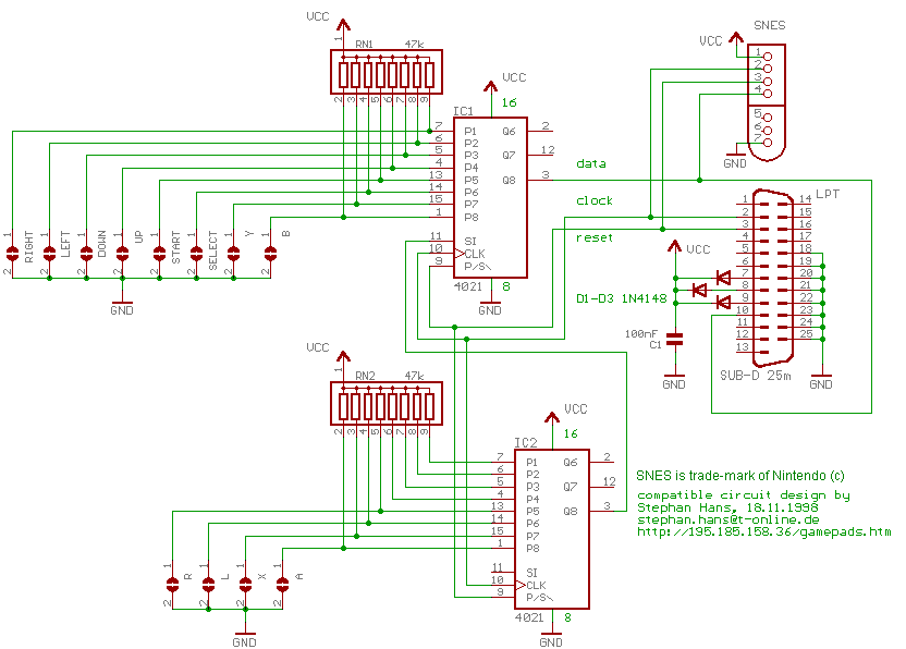
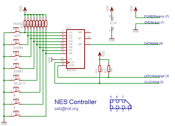
http://www.gamesx.com/controldata/nessnes.htm

My goal was to connect my custom db15 neogeo compatible controller to the snes by using one of the above scenarios, so far without success. Unfortunately I have no idea what im missing here. Both scenarios are not working for me and i have no idea what may be the cause (assuming the schematics are fine). I very quickly made simple one sided boards in eagle, take a look at it, maybe You will find some flaws in it:

Attachment:
File comment: Eagle schematics
snes_controller.zip [52.69 KiB]
Downloaded 288 times


Both controllers act the same, only "B" button is working fine, other buttons are not working at all. The strange thing is - when I hold the B button, im able to use left, right, start, select and A buttons - I wonder if schematics found on the web are correct, or maybe I made some mistakes while designing that simple boards. I have already build an arcade controller for NES and Sega MD without bigger issues.

Looking forward for some help!
Re: SNES controller schematic
by on (#141762)
hyvax wrote:
Both controllers act the same, only "B" button is working fine, other buttons are not working at all. The strange thing is - when I hold the B button, im able to use left, right, start, select and A buttons - I wonder if schematics found on the web are correct, or maybe I made some mistakes while designing that simple boards
That sounds kinda like the B button is shorted to P/S. Or at least, something is definitely wrong with IC1's P/S pin, anyway.
Re: SNES controller schematic
by on (#141801)
This is the sch I use (works of course).
this is for a single controller. so for 2 controllers, you'd need x 2.

Edit: resistor network is 10k value
Re: SNES controller schematic
by on (#141822)
Thanks for posting guys - looks like schematics are OK, after checking on the one You posted Markfrizb... according to the schema You posted - just to be 100% sure:

Image

1) +5V
2) Clock
3) Latch (P/S)
4) Data (Dataout)
7) GND

is this correct? If Yes I still have no clue what I'm missing here :(
Re: SNES controller schematic
by on (#141824)
I don't have Eagle so I can't view your files.
Re: SNES controller schematic
by on (#141825)
PNG versions here:

whicker wrote:
I don't have Eagle so I can't view your files.
Re: SNES controller schematic
by on (#141836)
hyvax wrote:
Thanks for posting guys - looks like schematics are OK, after checking on the one You posted Markfrizb... according to the schema You posted - just to be 100% sure:

Image

1) +5V
2) Clock
3) Latch (P/S)
4) Data (Dataout)
7) GND

is this correct? If Yes I still have no clue what I'm missing here :(


Yes, that's correct
Re: SNES controller schematic
by on (#141860)
Good news :D while looking for the answer and a possible solution to the problem I found this schematic on the web:

http://arcadecontrols.com/images/stephan_snes_cc.gif

it caught my attention, that not used "SI" pin11 on the 2nd 4021 is not grounded there, so I tried it and un-grounded this pin in my circuit... and everything is working like a charm now! That did the trick.

So... I guess (in mine experience) that unused serial data input on the 2nd 4021 should not be grounded ! Any idea why on almost every schematic on the web it is? Strange...
Re: SNES controller schematic
by on (#142019)
so what happens if you pull that SI pin up to +5V instead of leaving it floating?
Re: SNES controller schematic
by on (#142039)
That SI pin is not "not used". It is used to define the padding bits that appear after reading the first 16 bits. That bits are used for detecting if a controller is connected - and as far as I can tell they should be LOW, so GNDing that pin was correct.

When not GNDing it, at least some games should stop working (if they contain a controller detection function). I don't know why your circuit worked better without GNDing - unless maybe you did have shortcut SI with some nearby pin(?).

Aside from that, if you want to use the circuit on a PAL console, then you will need pull-up resistors on the open-collector outputs from SNES side, ie. on the CLK and LATCH lines.

Maybe... if you are using a PAL console, then your floating open-collectors signals might have been "healed" by leaving SI floating, too. But of course, relying on floating signals wouldn't be a good solution.
Re: SNES controller schematic
by on (#142042)
nocash wrote:
That SI pin is not "not used". It is used to define the padding bits that appear after reading the first 16 bits. That bits are used for detecting if a controller is connected - and as far as I can tell they should be LOW, so GNDing that pin was correct.

When not GNDing it, at least some games should stop working (if they contain a controller detection function). I don't know why your circuit worked better without GNDing - unless maybe you did have shortcut SI with some nearby pin(?).

Aside from that, if you want to use the circuit on a PAL console, then you will need pull-up resistors on the open-collector outputs from SNES side, ie. on the CLK and LATCH lines.

Maybe... if you are using a PAL console, then your floating open-collectors signals might have been "healed" by leaving SI floating, too. But of course, relying on floating signals wouldn't be a good solution.


Thanks for that explanation nocash!

Im using this circuit on a PAL console :) so far every game i tried works OK and detected the controller without any issues. I already tried putting pullups on clk and latch lines (with grounded 2nd SI line) while trying possible solutions to the problem. Pullups just like I did in the NES controller, according to this schema:

https://projects.drogon.net/wp-content/uploads/2012/08/nes-controller-schematic.png

and it was not working :) - to be honest I have no idea why it works with floating 2nd SI... double checked on a original PAL SNES controller - this pin IS grounded, no doubt about that. I already checked for shorted lines like 10x times, and Im 100% sure everything is connected as it should.

Maybe signal lines are to close to eachother on the PCB are interferencing somehow... no idea, im not that good in electronics. Also, IC's used in original controller from what I saw are 4021B - IC's that I put in mine are 4021N (not sure about that "N" - will check and confirm - anyway they differs) maybe some characteristics of that ICs differ... ?
Re: SNES controller schematic
by on (#183554)
hi all,

I ran into the exact same problem using multiple schematics from the web, so just the B button works, and refused to give up.. turns out that the exact value for the pull-up resistors for latch/data/clock is pretty important.

on a breadboard version of the schematics from raphael assenat, I ended up using a 1.2kohm resistor just on clock, and on an (identical) PCB version that I made the same value wouldn't even work, so I went down to 467ohm.. now everything is working consistently.

note that I use 10kohm pull-ups for all buttons. I also put a little bit of aluminum tape on the conductive little plates under the select and start buttons, or there was too much resistance in them. looks like this might be solvable as well by varying the 10kohm resistors, but I've had enough.. :-)

here's a link to my project, which also includes a precisely 3d-modeled and printed controller (electronics go inside):

http://www.thingiverse.com/thing:337896

I hope to write a detailed summary of this project on my blog soon:

http://blogfarts.blogspot.nl/