NSS (Super System) -- anyone know the pin out of the slots?

This is an archive of a topic from NESdev BBS, taken in mid-October 2019 before a server upgrade.
View original topic
NSS (Super System) -- anyone know the pin out of the slots?
by on (#117833)
Calling DogP ??????

I'm trying to determine what the pinout assignments are for the Super System card slots. DogP had them mapped out but has disappeared from this forum.
I BELIEVE NoCash would like to know as well to update his most excellent docs on the SNES and varients.
Re: NSS (Super System) -- anyone know the pin out of the slo
by on (#117894)
Can you find the service manual? I'm pretty sure I've viewed the schematic in the past, but I can't find it right now.
Re: NSS (Super System) -- anyone know the pin out of the slo
by on (#117906)
I know the service manual doesn't tell you the cartridge slot pinouts. Maybe you are thinking of the jamma (edge connector) pinout?? Trying to document the cartridge slots.
DogP determined that it was fully compatible for regular carts except for the CIC.
He was even in the process of making a converter so he could use regular carts.... Then he disappeared from the forums. Has anyone heard from him??
Re: NSS (Super System) -- anyone know the pin out of the slo
by on (#117908)
Mark has emailed me the pinout in .xls and .pdf format (I have no damn clue why). Anyway here it is:
Code:
100 pin (2x50) connector DINN
  bottom A          top B
  1  gnd            vpp  1
  2  gnd            vpp  2
  3  R3 then CIC7   CIC6 3
  4  R2 then CIC5   CIC8 4
  5  ..from NSS     CIC1 5
  6  d3             d4   6  ;\
  7  d2             d5   7  ;
  8  d1             d6   8  ;
  9  d0             d7   9  ;
  10 a0             CE/ 10  ;
  11 a1             a10 11  ; inst rom
  12 a2             OE/ 12  ;
  13 a3             a11 13  ;
  14 a4             a9  14  ;
  15 a5             a8  15  ;
  16 a6             a7  16  ;
  17 a12            gnd 17  ;/
  18 gnd            vpp 18
  19 gnd            vpp 19
  20 gnd            Vcc 20  ;\
  21 gnd            Vcc 21  ;
  22 n/c?           n/c 22  ;
  23 n/c?           n/c 23  ;
  24 n/c?           n/c 24  ;
  25 n/c?           n/c 25  ;
  26 n/c?           n/c 26  ;
  27 OE/       Sram WE/ 27  ;
  28 d3             d4  28  ; SNES bus
  29 d2             d5  29  ;
  30 d1             d6  30  ;
  31 d0             d7  31  ;
  32 n/c       ???A23?? 32  ;
  33 a0        ???A22?? 33  ;
  34 a1             A21 34  ;
  35 a2             A20 35  ;
  36 a3             a19 36  ;
  37 a4             a18 37  ;
  38 a5             a17 38  ;
  39 a6             a16 39  ;
  40 a7             a15 40  ;
  41 a8      hi-lo roms 41  ;
  42 a9             a14 42  ;
  43 a10            a13 43  ;
  44 a11            a12 44  ;/
  45 n/c            n/c 45
  46 n/c                46
  47                n/c 47
  48 n/c      *Sram CE2 48
  49 gnd            Vcc 49
  50 gnd            Vcc 50

Looks as if one could easily guess the missing pins. But would be nice if somebody could verify them on a real NSS mainboard:
    * A23-A15 are most likely on pins 33..41 (not pins 32..42)?
    * Pins 20..48 seem to be arranged identically as on SNES cartridges (but without the CIC and supply pins)?
    * Pin 5.A might be the slot select signal (if so, it should be different signal on each of the three slots)?
    * Vpp is... what? Presumably not prom/eprom programming voltage... so what is it... why is it called Vpp?
    * The "CICn" signals do refer to "pin n" of the 8pin Prom chip, is that correct?
EDIT: After checking some photos... above pinout is somehow mirrored... showing the pinout as when gazing at solder side of the mainboard.
EDIT2: After checking more photos... oops, above was just right... showing the pinput as when gazing at the component side of the mainboard.
Re: NSS (Super System) -- anyone know the pin out of the slo
by on (#118049)
Ah, maybe I was confusing it with the Playchoice schematic. I've seen the pinout before, but it probably was the one posted.

I can't say if he's disappeared from there too because I don't follow things much anymore, but another place to check for DogP would be the KLOV forums.
Re: NSS (Super System) -- anyone know the pin out of the slo
by on (#118090)
nocash wrote:
* The "CICn" signals do refer to "pin n" of the 8pin Prom chip, is that correct?

Thats correct, I verified it on a super mario world board
Re: NSS (Super System) -- anyone know the pin out of the slo
by on (#118130)
Thanks for checking the PROM pin connection!

Here's how the complete pinout is supposed to look like:

Code:
             Solder side   Component side
                      A    B
                  GND - 50 - VCC                                ;\
                  GND - 49 - VCC                                ;
  CPU.48   ?  MCK 21M - 48 - /WRAMSEL ?  WRAM.15                ;
          ??   EXPAND - 47 - REFRESH  ?  WRAM.7                 ;
  WRAM.47  ?      PA6 - 46 - PA7      ?  WRAM.50                ;
  WRAM.56  ?    /PARD - 45 - /PAWR    ?  WRAM.58                ;
                  A11 - 44 - A12                                ;
                  A10 - 43 - A13                                ;
                   A9 - 42 - A14                                ;
                   A8 - 41 - A15      ?  WRAM.38                ;
                   A7 - 40 - A16      ?  WRAM.40                ; SNES
                   A6 - 39 - A17      ?  CPU.11                 ;
                   A5 - 38 - A18      ?  CPU.12                 ;
                   A4 - 37 - A19      ?  CPU.13                 ;
                   A3 - 36 - A20      ?  CPU.14                 ;
                   A2 - 35 - A21      ?  CPU.15                 ;
                   A1 - 34 - A22      ?  WRAM.42                ;
                   A0 - 33 - A23      ?  CPU.17                 ;
  CPU.46   ?     /IRQ - 32 - /ROMSEL  ?  CPU.77                 ;
                   D0 - 31 - D4       ?? WRAM.2   ;\            ;
                   D1 - 30 - D5       ?? WRAM.3   ; or D4..D7   ;
                   D2 - 29 - D6       ?? WRAM.4   ; reversed?   ;
                   D3 - 28 - D7       ?? WRAM.5   ;/            ;
                  /RD - 27 - /WR                                ;
  WRAM.8   ?   /RESET - 26 - SYSCK    ?  WRAM.6                 ;
  WRAM.53  ?      PA0 - 25 - PA1      ?  WRAM.54                ;
  WRAM.43  ?      PA2 - 24 - PA3      ?  WRAM.44                ;
  WRAM.45  ?      PA4 - 23 - PA5      ?  WRAM.46                ;
  R96+C28 ??  SOUND-L - 22 - SOUND-R  ?? R95+C25                ;
                  GND - 21 - VCC                                ;
       _________  GND - 20 - VCC  _______________________       ;/
                  GND - 19 - VPP      ?  WRAM.1                 ;\
                  GND - 18 - VPP      ?  WRAM.1                 ;
  INST.2   ??     A12 - 17 - GND      ?  WRAM.64                ;
  INST.4    ?      A6 - 16 - A7       ?? INST.3                 ;
  INST.5    ?      A5 - 15 - A8       ?  INST.25                ;
  INST.6    ?      A4 - 14 - A9       ?  INST.24                ;
  INST.7    ?      A3 - 13 - A11      ?  INST.23                ; INST ROM
  INST.8    ?      A2 - 12 - /OE      ?? INST.22                ;
  INST.9    ?      A1 - 11 - A10      ?  INST.21                ;
  INST.10   ?      A0 - 10 - /CE      ?? INST.20                ;
  INST.11   ?      D0 - 9  - D7       ?  INST.19                ;
  INST.12   ?      D1 - 8  - D6       ?  INST.18                ;
  INST.13   ?      D2 - 7  - D5       ?  INST.17                ;
  INST.15  ??      D3 - 6  - D4       ?  INST.16                ;/
  from NSS ??  /SLOTn - 5  - PROM.DTA                           ;\
    via R2 - PROM.TST - 4  - PRIM.CNT                           ;
    via R3 - PROM.RES - 3  - PROM.CLK                           ; PROM
                  GND - 2  - VPP      ?  WRAM.1                 ;
                  GND - 1  - VPP      ?  WRAM.1                 ;/


The guessed pins are marked with question marks, with the assumed numbers on S-CPU, S-WRAM chips (on mainboard), and INST-ROM chips (on cartridge), or Rnn/Cnn resistors (on mainboard, assuming it uses same numbering as normal SNES consoles). It was quite some work to compile that list - would be glad if somebody could verify it! If it's right then you should see a 0 ohm connection between the cartridge pins and chip pins.
Re: NSS (Super System) -- anyone know the pin out of the slo
by on (#118290)
No problem :)
I didn't have much time tonight and I only had my iPad so it was quite hard to document...
Anyway I started to check the question marks but some of your suggestions doesn't match with my board

!? Or ?! Means correct
n? Or ?n means no connection
Cpu#! Means it is a connection to this pin instead

nocash wrote:
Code:
             Solder side   Component side
                      A    B
                  GND - 50 - VCC                                ;\
                  GND - 49 - VCC                                ;
  CPU.48   ?!  MCK 21M - 48 - /WRAMSEL ?  WRAM.15                ;
          ??   EXPAND - 47 - REFRESH  ?  WRAM.7                 ;
  WRAM.47  ?n      PA6 - 46 - PA7      ?  WRAM.50                ;
  WRAM.56  ?n    /PARD - 45 - /PAWR    ?  WRAM.58                ;
                  A11 - 44 - A12                                ;
                  A10 - 43 - A13                                ;
                   A9 - 42 - A14                                ;
                   A8 - 41 - A15      ?  WRAM.38                ;
                   A7 - 40 - A16      ?  WRAM.40                ; SNES
                   A6 - 39 - A17      ?  CPU.11     Cpu9!            ;
                   A5 - 38 - A18      ?  CPU.12      Cpu10!           ;
                   A4 - 37 - A19      ?  CPU.13      Cpu11!           ;
                   A3 - 36 - A20      ?  CPU.14                 ;
                   A2 - 35 - A21      ?  CPU.15                 ;
                   A1 - 34 - A22      ?  WRAM.42                ;
                   A0 - 33 - A23      ?  CPU.17                 ;
  CPU.46   !?     /IRQ - 32 - /ROMSEL  ?  CPU.77                 ;
                   D0 - 31 - D4       ?? WRAM.2   ;\            ;
                   D1 - 30 - D5       ?? WRAM.3   ; or D4..D7   ;


To be continued...
Re: NSS (Super System) -- anyone know the pin out of the slo
by on (#118393)
Okay, then at least MCK and /IRQ are same as on normal SNES carts. That makes it surprising that PA6 and /PARD aren't same, too.
And A17,A18,A19... are you sure they are wired like that? It doesn't match with normal SNES cart layout, and doesn't match with Mark's NSS pinouts (no matter if he were referring to the LoROM memory chip address lines, or to the actual console address lines).
Btw. testing the WRAM pins should be easiest, as they larger than the ROM pins.
Re: NSS (Super System) -- anyone know the pin out of the slo
by on (#118404)
If this makes any difference, I hand wired a NSS cart to be hi-rom (cause all the NSS carts are all lo rom) and it worked well. So when I mapped out the rom info, yes, it was mapped as lo rom.
Re: NSS (Super System) -- anyone know the pin out of the slo
by on (#118836)
nocash wrote:
Okay, then at least MCK and /IRQ are same as on normal SNES carts. That makes it surprising that PA6 and /PARD aren't same, too.
And A17,A18,A19... are you sure they are wired like that? It doesn't match with normal SNES cart layout, and doesn't match with Mark's NSS pinouts (no matter if he were referring to the LoROM memory chip address lines, or to the actual console address lines).

Sorry, my bad, I'll post a updated version soon-ish
Re: NSS (Super System) -- anyone know the pin out of the slo
by on (#118837)
Ok lets see...
Quote:
* A23-A15 are most likely on pins 33..41 (not pins 32..42)?
correct, A12..A23 is at B44..B33
Quote:
* Pins 20..48 seem to be arranged identically as on SNES cartridges (but without the CIC and supply pins)?
similar but not identically
Quote:
* Vpp is... what? Presumably not prom/eprom programming voltage... so what is it... why is it called Vpp?
"Vpp" is connected to pin 1 on inst rom which is, according to my datasheet for D27C256, actually is Vpp. However, pin1 on inst rom is also connected to pin28 which is Vcc. So it should probably be called Vcc_instrom instead. You can see that the pcb is actually divided on the top layer into two Vcc planes, just where you have a line in your pinout.

I've have only had the time to check the B side yet, and it can be found here (sorry for writing in a spread sheet, but it can be quite nice some time)

I'll continue with side A and write a line here when I'm done.
Oh, and feel free to copy/share/include it in your doc if you like
Re: NSS (Super System) -- anyone know the pin out of the slo
by on (#118848)
Cool. If some of the outer pins are arranged differently as on SNES, and pin 48.B is /RESET then it makes a lot more sense that Mark said that it connects to sram CE2.

Also thanks for verifying that D4..D7 are ordered opposite as on SNES (I was thinking it might have been a typo, but now it's double checked).

How are that two VCC's from SNES and INST-ROM wired on the Mainboard? Are they just short-cut with each other, or somehow decoupled via loops, or are they actually wired to different power sources? Or are they even wired to transistors or relays - allowing to power-down the cartridge's SNES chips for example?

And when powered, they are both +5V, aren't they? At least the SNES should get 5V. And the INST-ROM EPROM also looks like 5V component on photos.
Re: NSS (Super System) -- anyone know the pin out of the slo
by on (#118865)
Both the inst rom and the z80 is 5v components so it should be 5v but I don't have access to any jamma cabinet or psu for that matter either so I can't plug it in and check.

I guess it would make sense to have some kind of low pass filter between the different CPUs but I cannot remember any coil/inductor (if that's what you mean by loops). But I'll look into it when I map out the A side.
Re: NSS (Super System) -- anyone know the pin out of the slo
by on (#119034)
I reached out to DogP on the KLOV forums asking him about the NSS slot pinouts.
He has not returned my PM's.
Anyone here have a better relationship with him that he might answer??

He knows what the pinouts are..... And he left this forum a long time ago.
Re: NSS (Super System) -- anyone know the pin out of the slo
by on (#119040)
Markfrizb wrote:
I reached out to DogP on the KLOV forums asking him about the NSS slot pinouts.
He has not returned my PM's.
Anyone here have a better relationship with him that he might answer??

He knows what the pinouts are..... And he left this forum a long time ago.

Did you even read nocash's post? "Mark has emailed me the pinout in .xls and .pdf format (I have no damn clue why). Anyway here it is"


DERP, I thought Mark was DogP's name... my bad as always :oops:
Re: NSS (Super System) -- anyone know the pin out of the slo
by on (#119042)
I am afraid that you've misread my post. The pinouts were emailed from markfrizb. I don't know if dogp has more complete pinouts.
Re: NSS (Super System) -- anyone know the pin out of the slo
by on (#119043)
DogP has a complete pinout. He had a yoshi's island cart running on a NSS with a converter he built.
He had to add a CIC-lock for the snes games that looked to the CIC for an unlock.

He pm me long ago when he was working on it....
Re: NSS (Super System) -- anyone know the pin out of the slo
by on (#123171)
Hey, I thought this would be some small afternoon project, but now it's a four month project without end in sight! I understand that it may be a bit uncomfortable to reverse-engineer clumsy arcade cabinets and that you may need strong torches and other cave exploration equipment (if you don't have the mainboard laying on your table). Still, there are only a handful of unknown pins left, so how difficult could it be to get them tracked down?

For reference, here's the complete list of currently known pins (and guessed/unknown pins with question marks):
Code:
             Solder side   Component side
                      A    B
                  GND - 50 - VCC                                ;\
                  GND - 49 - VCC                                ;
  CPU.48   ?  MCK 21M - 48 - /RESET      WRAM.8                 ;
  WRAM.7 ? ??         - 47 - SYSCLK      WRAM.6                 ;
  WRAM.7 ? ??         - 46 -          ?? WRAM.7 ?               ;
  WRAM.7 ? ??         - 45 - /WRAMSEL    WRAM.15                ;
                  A11 - 44 - A12         CPU.6                  ;
                  A10 - 43 - A13         CPU.7                  ;
                   A9 - 42 - A14         CPU.8                  ;
                   A8 - 41 - A15         CPU.9                  ;
                   A7 - 40 - A16         CPU.10                 ;
                   A6 - 39 - A17         CPU.11                 ; SNES
                   A5 - 38 - A18         CPU.12                 ;
                   A4 - 37 - A19         CPU.13                 ;
                   A3 - 36 - A20         CPU.14                 ;
                   A2 - 35 - A21         CPU.15                 ;
                   A1 - 34 - A22         CPU.16                 ;
                   A0 - 33 - A23         CPU.17                 ;
  CPU.46   ?     /IRQ - 32 - /ROMSEL     CPU.77                 ;
                   D0 - 31 - D7          WRAM.5   ;\D4..D7 in   ;
                   D1 - 30 - D6          WRAM.4   ; opposite    ;
                   D2 - 29 - D5          WRAM.3   ; order as    ;
                   D3 - 28 - D4          WRAM.2   ;/on SNES     ;
                  /RD - 27 - /WR         WRAM.59                ;
  WRAM.53  ?      PA0 - 26 - PA1         WRAM.54                ;
  WRAM.43  ?      PA2 - 25 - PA3         WRAM.44                ;
  WRAM.45  ?      PA4 - 24 - PA5         WRAM.46                ;
  WRAM.47  ?      PA6 - 23 - PA7         WRAM.50                ;
  WRAM.56  ?    /PARD - 22 - /PAWR       WRAM.58                ;
                  GND - 21 - VCC                                ;
  ______________  GND - 20 - VCC  ___________________           ;/
                  GND - 19 - VPP                                ;\
                  GND - 18 - VPP      ?  WRAM.1 ?               ;
  INST.2          A12 - 17 - GND      ?  WRAM.64 ??             ;
  INST.4           A6 - 16 - A7          INST.3                 ;
  INST.5           A5 - 15 - A8          INST.25                ;
  INST.6           A4 - 14 - A9          INST.24                ;
  INST.7           A3 - 13 - A11         INST.23                ; INST ROM
  INST.8           A2 - 12 - /OE         INST.22                ;
  INST.9           A1 - 11 - A10         INST.21                ;
  INST.10          A0 - 10 - /CE         INST.20                ;
  INST.11          D0 - 9  - D7          INST.19                ;
  INST.12          D1 - 8  - D6          INST.18                ;
  INST.13          D2 - 7  - D5          INST.17                ;
  INST.15          D3 - 6  - D4          INST.16                ;/
  from NSS ??  /SLOTn - 5  - PROM.DTA    PROM.1                 ;\
  PROM.5-R2  PROM.TST - 4  - PROM.CNT    PROM.8                 ;
  PROM.7-R3  PROM.RES - 3  - PROM.CLK    PROM.6                 ; PROM
                  GND - 2  - VPP                                ;
                  GND - 1  - VPP                                ;/


Component Side (B) is mainly complete, based on mark's original info and additional info from hyarion; https://docs.google.com/spreadsheet/ccc ... QNmc#gid=0 - I've kept only two question marks on VPP/GND pins, both related to the connection on the MAINBOARD side (not on the cartridge side):
For VPP on Pin 1/2/18/19.B: it would be interesting if does have some 0 ohm connection to VCC (or maybe 1 or 2 ohms in case it goes through a inductor).
For GND on Pin 17.B: this pin isn't following the arrangement of the other supply pins, ie. if it is NOT wired to GND on the mainboard side then it might be something else (like a muted audio input, a cartridge_connected signal, or some other unused/reserved/special stuff).

Solder Side (A) This is still having some question marks. Though I've removed the ones on the INST.ROM pins (mark's specs on A7 and A12 looked a bit messy to be, but since hyarion has verified A7, I will trust that nintendo did really have them arranged like that).
The MCK and /IRQ have been already confirmed here: viewtopic.php?p=118290#p118290 (but hyarion did strike-out the text, so dunno of they are still confirmed or not).
The PA0, PA2, PA4, PA6, /PARD pins are guessed; based on the PA1,PA3,PA5,PA7,/PAWR pin arrangement on Side B.

Missing Pins Pin 47.A, 46.A, 45.A, 46.B aren't assigned yet. But they might correspond to SNES pins REFRESH, EXPAND, SOUND-L and SOUND-R.
I would assume that one of them is really REFRESH (WRAM.7).
SOUND-L/R might be also supported, but might be hard to verify since the signals might get routed through capacitors before reaching the audio amplifier - on the other hand, such capacitor routing would be hinting on audio stuff.
And EXPAND, well, that would go to the SNES expansion port, which doesn't exist in the NSS. So the fourth unknown pin might be NC, or it might have completely different function as in SNES.

Slot Selection this might exceed to what-pin-is-there question. But then, the NSS is a multicart system, so it would be pointless to reverse-engineer the NSS pinouts without understanding the slot selection.
Current theory is that Pin 5.A might be a /SLOTn select signal (actually three signals, /SLOT1, /SLOT2, /SLOT3, for the three cartridge slots respectively). However that theory is solely based on mark's description, saying that Pin 5.A is "from NSS" (don't ask why that made me think that it might be a slot selection signal, I was just guessing - and somewhere, such a signal should exist).

And finally, it would be important to know how that supposed /SLOTn signal is used. Juding from PCB photos, it looks same/similar as in Playchoice 10, ie. probably using the 74xx367 chip to disable the SNES and INSTROM and PROM chipselect signals when the cartridge slot isn't used.

EDIT/PS. The white 2x50 pin connector on the NSS cartridges does look as if might be some standard component. On photos it does even look as if there might be some part number on that connectors. Only problem is that Nintendo has covered that part number underneath of a sticker. Just a suggestion for another expert hacking project: Somebody try removing that sticker.
Re: NSS (Super System) -- anyone know the pin out of the slo
by on (#124231)
DogP has mailed me the NSS pinout (plus some info on connector names, supply pins, and slot selection). First of, here's the pinout, this confirms the known pins & guessed pins & solves the missing pins:
Attachment:
NSS_Pinout_by_DogP.jpg
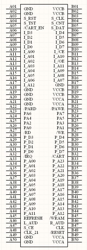
NSS_Pinout_by_DogP.jpg [ 107.57 KiB | Viewed 1271 times ]

The P_xxx pins are SNES Program ROM, the I_xxx pins are INST ROM, the S_xxx pins are Security PROM, of which, the S_CE pin is a bit far away from the other PROM pins (no idea why Nintendo did arrange like that), and it should be actually called /S_CE (as it's active low, according to RP5H01 datasheet).

In plain ASCII, the pin-out should look as so:
Code:
Cartridge Slots (3 slots, 2x50pin each)
            Solder side    Component side
                      A    B
  WRAM.64         GND - 1  - VCC2        INST.28                ;\
  WRAM.64         GND - 2  - VCC2        INST.28                ; PROM
  PROM.7-R3  PROM.RES - 3  - PROM.CLK    PROM.6                 ; (and SNES
  PROM.5-R2  PROM.TST - 4  - PROM.CNT    PROM.8                 ; select)
              /SNES_# - 5  - PROM.DTA    PROM.1                 ;/
  INST.15          D3 - 6  - D4          INST.16                ;\
  INST.13          D2 - 7  - D5          INST.17                ;
  INST.12          D1 - 8  - D6          INST.18                ;
  INST.11          D0 - 9  - D7          INST.19                ;
  INST.10          A0 - 10 - /CE_#       INST.20                ;
  INST.9           A1 - 11 - A10         INST.21                ; INST ROM
  INST.8           A2 - 12 - /OE         INST.22                ;
  INST.7           A3 - 13 - A11         INST.23                ;
  INST.6           A4 - 14 - A9          INST.24                ;
  INST.5           A5 - 15 - A8          INST.25                ;
  INST.4           A6 - 16 - A7          INST.3                 ;
  INST.2          A12 - 17 - GND         WRAM.64                ;
  WRAM.64         GND - 18 - VCC2        INST.28                ;
  WRAM.64 _______ GND - 19 - VCC2 ______ INST.28                ;/
  WRAM.64         GND - 20 - VCC         WRAM.1                 ;\
  WRAM.64         GND - 21 - VCC         WRAM.1                 ;
  WRAM.56       /PARD - 22 - /PAWR       WRAM.58                ;
  WRAM.47         PA6 - 23 - PA7         WRAM.50                ;
  WRAM.45         PA4 - 24 - PA5         WRAM.46                ;
  WRAM.43         PA2 - 25 - PA3         WRAM.44                ; SNES Bus
  WRAM.53         PA0 - 26 - PA1         WRAM.54                ; (and PROM
  WRAM.57         /RD - 27 - /WR         WRAM.59                ; select)
  WRAM.63          D3 - 28 - D4          WRAM.2   ;\D4..D7 in   ;
  WRAM.62          D2 - 29 - D5          WRAM.3   ; opposite    ;
  WRAM.61          D1 - 30 - D6          WRAM.4   ; order as    ;
  WRAM.60          D0 - 31 - D7          WRAM.5   ;/on SNES     ;
  CPU.46         /IRQ - 32 - /ROMSEL     CPU.77                 ;
  CPU.93           A0 - 33 - A23         CPU.17                 ;
  CPU.94           A1 - 34 - A22         CPU.16                 ;
  CPU.95           A2 - 35 - A21         CPU.15                 ;
  CPU.96           A3 - 36 - A20         CPU.14                 ;
  CPU.97           A4 - 37 - A19         CPU.13                 ;
  CPU.98           A5 - 38 - A18         CPU.12                 ;
  CPU.99           A6 - 39 - A17         CPU.11                 ;
  CPU.100          A7 - 40 - A16         CPU.10                 ;
  CPU.2            A8 - 41 - A15         CPU.9                  ;
  CPU.3            A9 - 42 - A14         CPU.8                  ;
  CPU.4           A10 - 43 - A13         CPU.7                  ;
  CPU.5           A11 - 44 - A12         CPU.6                  ;
  WRAM.7      REFRESH - 45 - /WRAMSEL    WRAM.15                ;
              AUDIO_L - 46 - AUDIO_R                            ;
  PROM.2   PROM./CE_# - 47 - SYSCLK      WRAM.6                 ;
  CPU.48      MCK 21M - 48 - /RESET      WRAM.8                 ;
  WRAM.64         GND - 49 - VCC         WRAM.1                 ;
  WRAM.64         GND - 50 - VCC         WRAM.1                 ;/
The NSS motherboard uses female Matsushita AXD100271 connectors, and the NSS
cartridges have male Matsushita AXD200251 connectors. Both are obsolete as of a
few years ago, but they're just shrouded 0.1" headers.


All pins are same on all three cartridge slots, except three pins have separate signals per slot:
A47: PROM./CE_# = PROM chip enable for slot 1,2,3 (can be directly wired to PROM)
B10: INST./CE_# = INST ROM chip enable for slot 1,2,3 (can be directly wired to EPROM)
A5: /SNES_# = SNES enable for slot 1,2,3 (must by manually ORed with /ROMSEL (and other pins if needed))

For the supply pins, B17 is actually GND (including on mainboard side). And for VCC pins: The Z80 supply (for INST ROM and PROM) is always powered, and the SNES supply can be switched off (via Q1 transistor on mainboard) (whatever that is good for, it might save some energy during menu selections, but during Demo mode the SNES supply needs to be certainly enabled).

About the /SNES_# signal (pin A5), basically this should be ORed with the SNES read/write/chip_select signals. Instead of using an OR gate, the NSS cartridges are usually doing this by using 74HC367 tri-state buffer (similar as PC10 carts), this chip could switch up to 6 signals (which may be actually required for some cartridges), but in normal NSS carts it is merely switching one single signal (/ROMSEL); wired as so: Pin1=/SNES_#, Pin2=/ROMSEL_IN (from NSS), Pin3=/ROMSEL_OUT (to cartridge; with pull-up resistor), all other inputs are GNDed, and all other outputs are NC.

Aside from /ROMSEL, it may be also required to switch /RD, /WR, /PARD, /PAWR, and in opposite direction: /IRQ. Together with the /ROMSEL signal, this could be done neatly via the six channels of the 74HC367 chip (plus six pull-up resistors).
/RD and /WR would be required for cartridges that do memory mapping without /ROMSEL=LOW (that would be: SRAM in HiROM carts, the NSS DIP switch cartridges, and several SNES coprocessor carts which do leave /ROMSEL completely unused).
/PARD and /PAWR would be needed only for making a 100% functional SNES adaptor (though in practice there aren't any SNES cartridges known to use that signals).
/IRQ might be required for some cartridges. If the cartridges do disable /IRQ upon /RESET, and if they do produce open-collector /IRQ signals then it wouldn't be required to disable /IRQ on deselected cartridges. But I've no idea if the existing SNES cartridges are really working like so (or maybe some do, and others don't). So it may be better to switch /IRQ by passing it through the 74HC367 (in opposite direction as the other signals, and with a pull-up resistor on the cartridge side (the resistor would be required for cartridges that do use open-collector /IRQ outputs) (for the NSS mainboard side: there should be already a pull-up resistor present, at least it's like so on SNES mainboards).

EDIT: A fully functional NSS-to-SNES-cartridge adaptor would also require a CIC chip (as a few SNES cartridges with special protections won't work if the 'console' doesn't output the correct CIC signals).
Accordingly, the adaptor would also need something that generates the 3.072MHz CIC clock signal (on a real SNES that would be 24.576MHz/8 coming from APU) (on the NSS adaptor it would require a separate oscillator, or if accuracy doesn't matter, then one might get away with 21.xxxMHz PAL/NTSC master clock divided by 7 (or dirtier: divided by 8)).
Unless there should be another way to get those protected cartridges to work (maybe by simply wiring CIC clock to VCC or GND, or by feeding it only a few dozen of CIC clks after reset, so it could initialize itself, but would never reach the point where the protection could do something harmful).