Does anybody know whether or not the MAD-1 toggles /CS on the SRAM for every address change, or does it just hold /CS low as long as the decoded address is in the SRAM region? I'm in the process of picking up some old abandoned projects now that I have a bit more time on my hands, and one of them is trying to use FRAM in place of SRAM. This guy was able to successfully use the FM1608 FRAM chip, but all I've been able to get my hands on are FM1608-B and FM16W08, which *should* still be compatible, but they just don't work, and I've beaten my head against the wall for countless hours trying to determine why, but to no avail. The only thing in the datasheet that really sticks out as "this could be the problem" is the fact that the Ramtron FRAM parts require a negative edge on the /CS line for every address change, unlike SRAM, which can change addresses any time that /CS is low. I have access to oscilloscopes, but not in a place where I could easily hook up a Super Nintendo while I'm probing... though I suppose I could blindly mash buttons without a TV and hope for the best, though that's probably not going to work so well. The only other difference I've found between the SRAM and FRAM is access times, which are only slightly different, and the overall cycle time is the same, just different setup/hold times. So anyway, back to my original question, does anybody know for certain whether or not the SRAM /CS line gets toggled for every access?
take a look at my old posting:
viewtopic.php?f=12&t=5886
the logic gate chips involved doing the chip select were the 74ALS series.
viewtopic.php?f=12&t=5886
the logic gate chips involved doing the chip select were the 74ALS series.
Did you try it with SRAM? If it doesn't work with SRAM then your problem isn't the FRAM. If it does work with SRAM then your line of questioning seems legit.
To answer your question, Strickly going off nocash's doc:
Those inputs on the truth table are the ONLY things that can affect your outputs. In the case of LOROM /ROMSEL must be low to access SRAM. I assume there's no way to keep /ROMSEL low from one cycle to the next. Therefore the SRAM /CE line MUST toggle from one access the the next. HIROM is a little less clear since /ROMSEL is high for SRAM accesses. In HIROM /CE is low ANYTIME those truth table entires hold true. So if NONE of those inputs change from one access to the next (which would seem possible but unlikely unless the CPU was operating from SRAM).
To simply answer your question is would seem that LoROM's SRAM /CE MUST toggle for every cycle, but not necessarily with HiROM. You'd have to confirm with the CPU opcodes, but I'd guess for typical load/stores from SRAM those inputs will change from one CPU cycle to the next making SRAM /CE cycle. This might not be the case if the CPU was operating from SRAM though...
To answer your question, Strickly going off nocash's doc:
Code:
MAD-1 Pinouts (Memory Address Decoder 1)
1 OUT1 /ROM.CS1 ;Chipselect to Upper ROM (NC if single ROM)
2 OUT2 /SRAM.CS ;Chipselect to SRAM
3 OUT3 /AUX.CS ;Chipselect to Expansion I/O or so (usually NC)
4 OUT4 /ROM.CS ;Chipselect to Single ROM (NC if two ROMs)
5 Vout ;Supply to SRAM (+3V when VCC=off, +5V when VCC=on)
6 VCC ;Supply from SNES (+5V)
7 Vbat ;Supply from Battery via resistor (+3V)
8 GND ;Supply Ground
9 IN6 /RESET ;From cart.26
10 IN5 MODE ;HiROM: VCC | LoROM: GND
11 IN4 /ROMSEL ;From cart.49
12 IN3 Addr3 ;HiROM: A22 (400000h) or A15 | LoROM: A22 (400000h) or VCC
13 IN2 Addr2 ;HiROM: A21 (200000h) | LoROM: A21 (200000h)
14 IN1 Addr1 ;HiROM: A14 (4000h) | LoROM: A20 (100000h)
15 IN0 Addr0 ;HiROM: A13 (2000h) | LoROM: A15 (8000h)
16 OUT0 /ROM.CS0 ;Chipselect to Lower ROM (NC if single ROM)
Note that Addr3 is sometimes wired this or that way. And, when using two ROMs, Addr2 is used as upper ROM address line (so the ROM-size may affect the SRAM/AUX mapping).
MAD-1 Logic Table
IN0 IN1 IN2 IN3 IN4 IN5 IN6 VCC vs --> Output being
Addr0 Addr1 Addr2 Addr3 /ROM MODE /RES Vbat dragged LOW
--------------------------------------------------------------------
HIGH x x x LOW LOW HIGH x --> /ROM.CS=LOW ;\
HIGH x LOW x LOW LOW HIGH x --> /ROM.CS0=LOW ;
HIGH x HIGH x LOW LOW HIGH x --> /ROM.CS1=LOW ; LoROM
LOW LOW HIGH HIGH LOW LOW HIGH x --> /AUX.CS=LOW ;
LOW HIGH HIGH HIGH LOW LOW HIGH VCC>Vbat --> /SRAM.CS=LOW ;/
x x x x LOW HIGH HIGH x --> /ROM.CS=LOW ;\
x x LOW x LOW HIGH HIGH x --> /ROM.CS0=LOW ;
x x HIGH x LOW HIGH HIGH x --> /ROM.CS1=LOW ; HiROM
HIGH HIGH LOW LOW HIGH HIGH HIGH x --> /AUX.CS=LOW ;
HIGH HIGH HIGH LOW HIGH HIGH HIGH VCC>Vbat --> /SRAM.CS=LOW ;/
Those inputs on the truth table are the ONLY things that can affect your outputs. In the case of LOROM /ROMSEL must be low to access SRAM. I assume there's no way to keep /ROMSEL low from one cycle to the next. Therefore the SRAM /CE line MUST toggle from one access the the next. HIROM is a little less clear since /ROMSEL is high for SRAM accesses. In HIROM /CE is low ANYTIME those truth table entires hold true. So if NONE of those inputs change from one access to the next (which would seem possible but unlikely unless the CPU was operating from SRAM).
To simply answer your question is would seem that LoROM's SRAM /CE MUST toggle for every cycle, but not necessarily with HiROM. You'd have to confirm with the CPU opcodes, but I'd guess for typical load/stores from SRAM those inputs will change from one CPU cycle to the next making SRAM /CE cycle. This might not be the case if the CPU was operating from SRAM though...
Yes, it definitely works with SRAM, I'm testing using donor carts with their SRAM removed, and I've tried re-inserting the SRAM to verify that it still works (it does). whicker, thanks for that link, I'll definitely read up on it. I'm glad to hear that it sounds like I was on the right track as far as the issue goes, and REALLY glad to hear that someone has gotten it working. I'll have to look at it some more, but can it be done using only the signals routed to the SRAM pinout? I'd love to make a nice drop-in replacement for original boards if possible. If not, no big deal...
Ok, so if I'm looking for a drop-in replacement module, I'd be using the correct memory size for the target board (64k or 256k... I don't have any 16k games worth the mod, but if I did, I'd just use a 64k chip and ground the upper address pins), so I don't need the AND gates on the address lines, only the glue logic on the /CE line. In your schematic, you're using the 74..139, but if I'm using it on a MAD-1 cart, what is the signal on the MAD-1 that corresponds to Y3 on the 139?
Alright, I managed to get it working! I didn't have any 7400 logic chips around, or any transistors, so I cheaped out and built the logic with diodes. Here's the schematic (forgive the use of the wrong kind of diodes in the schematic drawing, they were just plain old 1N4148 switching diodes). I used 330ohm resistors, couldn't find any information on what a good value would be, but 330 works. I would guess 10K would work, but I haven't tried it.

And here's the drop-in module (the same board works with FM1608 for 64K carts as well as FM1808 for 256K carts)

And here's the drop-in module (the same board works with FM1608 for 64K carts as well as FM1808 for 256K carts)
qwertymodo wrote:
I cheaped out and built the logic with diodes. Here's the schematic (forgive the use of the wrong kind of diodes in the schematic drawing, they were just plain old 1N4148 switching diodes). I used 330ohm resistors, couldn't find any information on what a good value would be, but 330 works. I would guess 10K would work, but I haven't tried it.
Um, wow. That's a huge amount of static power dissipation, as well as rather horrific transient behavior. You're putting a huge amount of load on whatever's generating your /OE, /WE, and /CE inputs. And ... 10kΩ resistors probably won't work; reverse-biased diodes are large enough capacitors that will exceed your timing requirements.
Just please don't do it again
It's all I had on hand... 
I'll be changing it to use 7400-based AND/OR gates before I order PCB's
I'll be changing it to use 7400-based AND/OR gates before I order PCB's
Ain't she purty?

Oh wow. It's beautiful... 
Actually that was pretty clever to use "DRL" gate technology (diode-resistor-logic?)
You probably will be able to use just one NOR or NAND package to come up with some sort of equivalent circuit.
Just do some research about the series you do pick (save some frustration and pick 5V ACT or ALS or better for this application).
For space, there are also super-tiny individual gate chips in 6 or 8 pin packages, but I haven't delved much into them. I bet you still can fit a normal 14-pin SMT logic gate chip on there.
Happy to have at least pointed you in the right direction
Sorry I don't reply fast enough. But you were on a roll there.
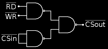
The TI SN74AHCT1G08 and SN74AHCT1G32 look perfect. Single-gate, and the AHCT series is TTL-input compatible (CMOS output). With the MAD-1 decoder, I only ended up needing 1 OR gate and 1 AND gate. Call the RAM /CS signal coming out of the MAD-1 CS_OUT and the /CS pin on the FRAM chip CS_IN:
CS_IN = CS_OUT | (RD & WR)
Now that I don't need the battery, the next step will be figuring out 32Mbit decoding without the MAD-1 (should be a breeze, I have plenty of info to work from), and then I'll have a full cart with off-the-shelf parts and non-volatile saves
CS_IN = CS_OUT | (RD & WR)
Now that I don't need the battery, the next step will be figuring out 32Mbit decoding without the MAD-1 (should be a breeze, I have plenty of info to work from), and then I'll have a full cart with off-the-shelf parts and non-volatile saves
You can build x OR (y AND z) by using three NAND gates (a single 7400). By deMorgan's law: (NOT X) NAND (Y NAND Z)
lidnariq wrote:
(NOT X) NAND (Y NAND Z)
That would also require an inverter to get NOT X, which is still 2 chips, so there isn't any real benefit. The 74..1GXX chips are single gates and they are TINY (which, to me, is a good thing... I guess if you don't like surface-mount soldering they would be awful, but you can also get the SOT-23 package, which isn't too bad).
NOT X is X NAND X ...
lidnariq wrote:
NOT X is X NAND X ...
derp... >.< it's been way too long since I've done discrete logic
Alright, how does this look? The SRAM256K part is the DIP-28 footprint, so the /CE line is the signal coming in from the decoder, and the CE with the bar over it is the actual pin on the FRAM chip. I probably could have better optimized the PCB layout by selecting which gates to hook up to what based on physical location, but the traces are simple enough I didn't bother.


Looks great.
As far as I can determine with my "chip being upside-down and rotated 180" sense, it appears to be wired correctly.
Like all unused gates, I'd just recommend you tie the two unused inputs of gate "D" to Vcc or Gnd. I'd recommend GND because I think you have a ground fill super close to those pins anyway.
The nice thing about EAGLE is that if the schematic is correct, it connects the PCB pins for you (you have to do the actual tracing, but it knows what's supposed to connect to what, so you can't accidentally connect 2 pins that aren't connected on the schematic or it yells at you). I'll go ahead and ground the unused gate inputs.
You wanted this circuit instead:
circuit.png [ 850 Bytes | Viewed 4300 times ]
For minimal routing difficulty, I'd probably either tie the 2nd (pins 4-5) NAND gate to ground or the 4th (pins 12-13) NAND gate to vcc.
Attachment:
circuit.png [ 850 Bytes | Viewed 4300 times ]
For minimal routing difficulty, I'd probably either tie the 2nd (pins 4-5) NAND gate to ground or the 4th (pins 12-13) NAND gate to vcc.
Good catch, I forgot NAND wasn't associative...
Hey whicker, how would you modify your schematic for a single, 16Mbit ROM? Where would you connect the ROM A20 line? Would you just hook it straight up to pin 46 on the cart edge? That's how the MAD-1 boards seem to do it... but the MAD-1 is decoded off of BA4 and BA5, where your schematic is decoding off of BA5 and BA6 (you call them CA21 and CA22). Also, would I then need glue logic between the 139 and the ROM /CS line? Y0 NAND Y1, maybe?
I'll answer this better tomorrow.
I just got back from anime central.
Yes A20 would just go from the chip to the cart edge.
You still need chip select logic so that the chip isn't always sending out data.
It's not Y0 nand Y1.
I just got back from anime central.
Yes A20 would just go from the chip to the cart edge.
You still need chip select logic so that the chip isn't always sending out data.
It's not Y0 nand Y1.
Alright, A20 from the flash chip goes to cart edge pin 46.
Chip Select on the flash chip would be the output from an OR gate:
Flash /CS = pin 49 (/ROMSEL) OR pin 47 (S-CPU A22)
In the exact diagram, you could also use the other half of the 74139 chip to make the OR function.
2A input tied to GND, 2B input still CA22, 2G still /ROMSEL, use output 2Y0 for chip select.
That's if you're actually using a 74139
whicker wrote:
Alright, A20 from the flash chip goes to cart edge pin 46.
Chip Select on the flash chip would be the output from an OR gate:
Flash /CS = pin 49 (/ROMSEL) OR pin 47 (S-CPU A22)
In the exact diagram, you could also use the other half of the 74139 chip to make the OR function.
2A input tied to GND, 2B input still CA22, 2G still /ROMSEL, use output 2Y0 for chip select.
That's if you're actually using a 74139
Chip Select on the flash chip would be the output from an OR gate:
Flash /CS = pin 49 (/ROMSEL) OR pin 47 (S-CPU A22)
In the exact diagram, you could also use the other half of the 74139 chip to make the OR function.
2A input tied to GND, 2B input still CA22, 2G still /ROMSEL, use output 2Y0 for chip select.
That's if you're actually using a 74139
I am using a 74139, but I'm trying to see if I can get all of the decoding working with just the 74139 and the 1 extra NAND gate I have available on the 7400.
So (just to talk this through and see if I'm getting this right):
ROM_CE = /CART OR A22 (/ROMSEL seems like a misnomer since when it's high, it disables both ROM and RAM, so it really acts as a /CARTSEL)
RAM_CE = (/CART OR (A21 NAND A22) OR A15) OR (/RD AND /WR)
Now, from the previous discussion, /CE can be simplified to
RAM_CE = NOT (/CART OR (A21 NAND A22) OR A15) NAND (/RD NAND /WR)
So, we build ROM_CE from the first half of the '139, and use the second half as a 3-input or for the (/CART OR (X) OR A15) where X is A21 NAND A22 (the 4th NAND gate).
If I actually got all of that right, this should do it...

After extensively looking at this, I can't find a reason why what you have wouldn't work.
The only caveat is that the FeRAM maps into banks 60h-6Fh as well as banks 70h-7Dh. I don't forsee this being a problem. Bank 6xh with A15=0 is ordinarily for the DSP-1 or whatever coprocessor for certain rom sizes. Shouldn't matter for what you're using it for.
The long chain of gates doesn't seem like it will glitch in a way to cause issues, and games are supposed to access Battery RAM in the slow speed area anyways.
Would there be a way to save maybe 1 or 2 nand gates? probably, but let's not worry about it.
I looked at your schematic again, and mine maps bank 6xh the same way yours does. Bank 6xh means BA5 and BA6 (A21/A22) are both high. In your schematic, that selects Y3 low, combined with A15 low selects RAM_CE unless both /RD and /WR are high.
qwertymodo wrote:
I looked at your schematic again, and mine maps bank 6xh the same way yours does. Bank 6xh means BA5 and BA6 (A21/A22) are both high. In your schematic, that selects Y3 low, combined with A15 low selects RAM_CE unless both /RD and /WR are high.
Yes, exactly.
I was okay with it not perfectly matching the mapping. It never caused issues (and it shouldn't). That area would be open bus otherwise.
I was trying to make the circuit have the bare minimum components to run, a goal you probably agree with.
I was just warning you of anything I knew was off, in case you were about to make a run of 10,000 of these or something.
Thanks for the help, guys. Just got the standalone PCB's in, and so far my Zelda: Parallel Worlds cart is working great with F-RAM on-board! 